

SGT device with silicon nitride barrier layer and method of making
A silicon nitride and barrier layer technology, applied in semiconductor/solid-state device manufacturing, semiconductor devices, electrical components, etc., can solve problems affecting system operation, device failure, etc., to solve problems such as unstable breakdown voltage, small threshold voltage, The effect of small on-resistance
- Summary
- Abstract
- Description
- Claims
- Application Information
AI Technical Summary
Problems solved by technology
Method used
Image

Examples
Embodiment
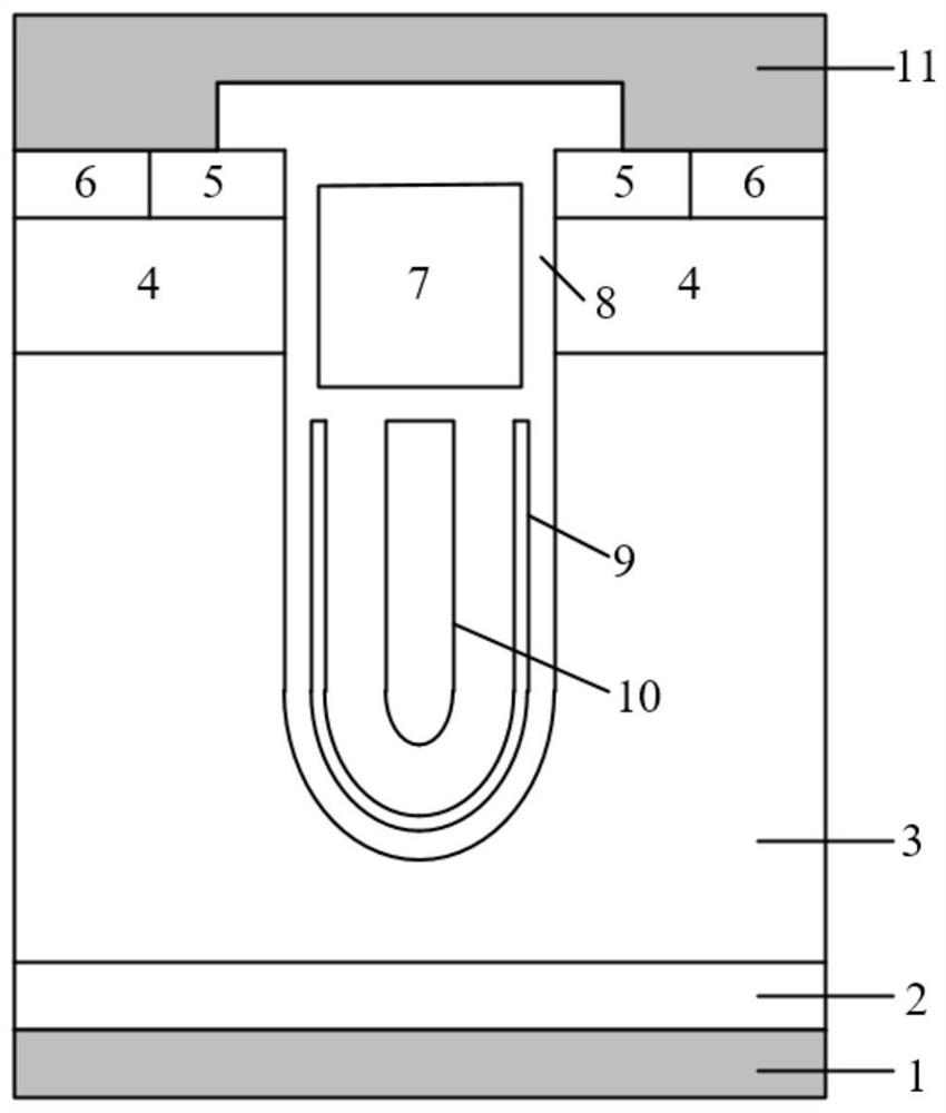
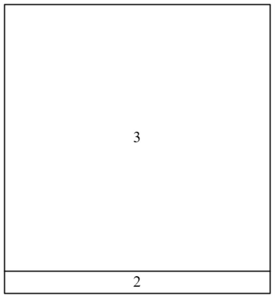
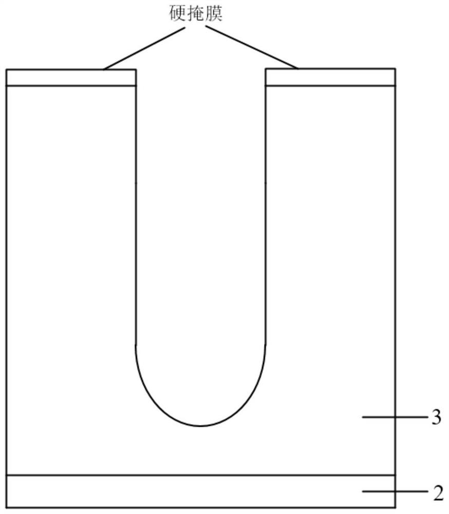
[0040] A SGT device with a silicon nitride barrier layer, characterized in that it includes a metallized drain 1, an N+ substrate 2, an N-drift region 3, and a metallized source 11 stacked sequentially from bottom to top;
[0041] The N-drift region 3 has a trench gate structure, a P-type doped region 4, a P+ heavily doped region 6 and an N+ heavily doped region 5;
[0042] The trench gate structure includes an oxide layer 8, a control gate electrode 7 located inside the oxide layer 8, a silicon nitride barrier layer 9 and a shielded gate electrode 10, and the silicon nitride barrier layer 9 and the shielded gate electrode 10 are located on the control gate electrode 7 Below, the control gate electrode 7 and the shielding gate electrode 10 are not in contact, the silicon nitride barrier layer 9 is U-shaped, and the silicon nitride barrier layer 9 is located in the oxide layer 8 on the left and right sides and the bottom of the shielding gate electrode 10;
[0043] The P-type d...
PUM
 Abstract
Description
Claims
Application Information