

Diode structure
a diode and structure technology, applied in the direction of basic electric elements, electrical equipment, semiconductor devices, etc., can solve the negative influence of the efficiency of the charge pump, and achieve the effect of reducing leakage current, improving performance, and increasing forward curren
- Summary
- Abstract
- Description
- Claims
- Application Information
AI Technical Summary
Benefits of technology
Problems solved by technology
Method used
Image

Examples
Embodiment Construction
[0026]The present invention will now be described with reference to the attached drawings to provide a thorough understanding. Furthermore, some system configurations and process steps are not disclosed in detail, as these should be well-known to those skilled in the art. Other embodiments maybe utilized, and structural, logical, and electrical changes may be made without departing from the scope of the present invention.
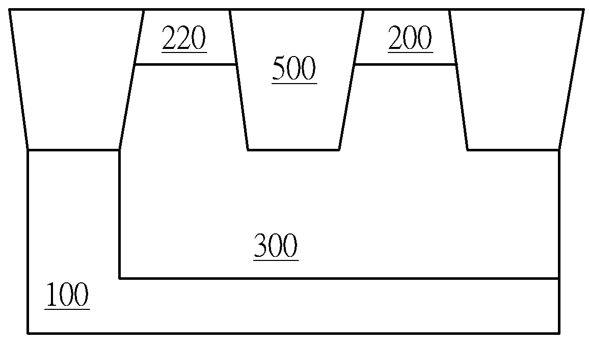
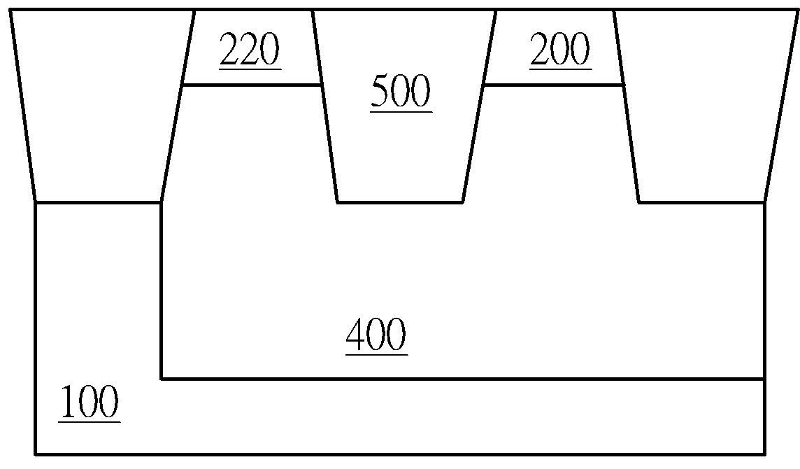
[0027]FIG. 1 and FIG. 2 are the schematic cross-sectional diagrams of two types of conventional diodes of the prior art.
[0028]Please refer to FIG. 1, which is the cross-sectional diagram of an N+ / PW diode. The heavily doped N+ doping region 200 and the P+ doping region 220 are disposed in the P well 300, and are separated by the isolation structure 500. When the diode is forward-biased, that is, when the electrical potential of the P+ doping region 220 is relatively positive with respect to the electrical potential of the N+ doping region 200, the potential barrier ...
PUM
 Abstract
Description
Claims
Application Information