
Schottky diode
A technology of Schottky diodes and regions, applied in the direction of electrical components, circuits, semiconductor devices, etc., can solve the problems of unfavorable electric field concentration effect and avalanche breakdown, so as to avoid the electric field concentration effect, increase the reverse breakdown voltage, Effect of Reducing Leakage Current
- Summary
- Abstract
- Description
- Claims
- Application Information
AI Technical Summary
Problems solved by technology
Method used
Image

Examples
Embodiment Construction
[0036] In order to make the features and advantages of the present invention more comprehensible, reference is made herein to Figure 4 A preferred example is described in detail as follows. However, the present invention should not be limited to implementation using the methods in the examples described below.
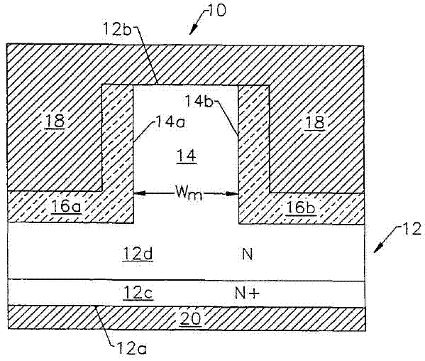
[0037] Figure 4 A cross-sectional structure diagram of the RC-TMBS designed according to the idea of the present invention is shown. The entire device is 5.6 μm wide and contains the following material layers from bottom to top:
[0038] The cathode 501 made of the first metal (Al in this example) has a thickness of 300 nm.
[0039] Heavy doping of the first conductivity type (in this case N-type) (in this case 1×10 20 cm -3 ) semiconductor (silicon Si in this example) 502 with a thickness of 300 μm.
[0040] Lightly doped (1×10 in this case) of the first conductivity type (N-type in this case) 16 cm -3 ) semiconductor (in this case, silicon Si) 503, plat...
PUM
| Property | Measurement | Unit |
|---|---|---|
| Doping concentration | aaaaa | aaaaa |
| Doping concentration | aaaaa | aaaaa |
| Width | aaaaa | aaaaa |
Abstract
Description
Claims
Application Information