Touch panel and manufacturing method thereof

A technology of a touch panel and a manufacturing method, which is applied in the direction of instruments, electrical digital data processing, and input/output process of data processing, etc., can solve problems such as electrode layer disconnection and height difference, and achieve reduction of electrode layer disconnection and good The effect of production yield

Active Publication Date: 2017-10-27
ACER INC
View PDF6 Cites 0 Cited by
  • Summary
  • Abstract
  • Description
  • Claims
  • Application Information

AI Technical Summary

Problems solved by technology

However, there is a height difference between the surface of the visual shielding layer in the non-display area and the surface of the display area
When the electrode layer is arranged on the surface of the visual shielding layer and the surface of the display area, the height difference between the visual shielding layer and the display area will easily lead to disconnection of the electrode layer

Method used


Image

  • Touch panel and manufacturing method thereof
  • Touch panel and manufacturing method thereof
  • Touch panel and manufacturing method thereof

Examples


Embodiment Construction

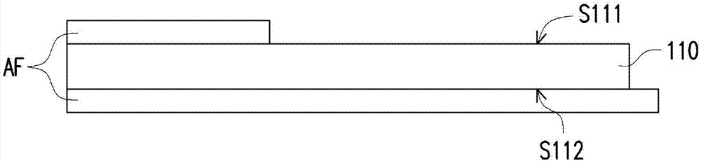
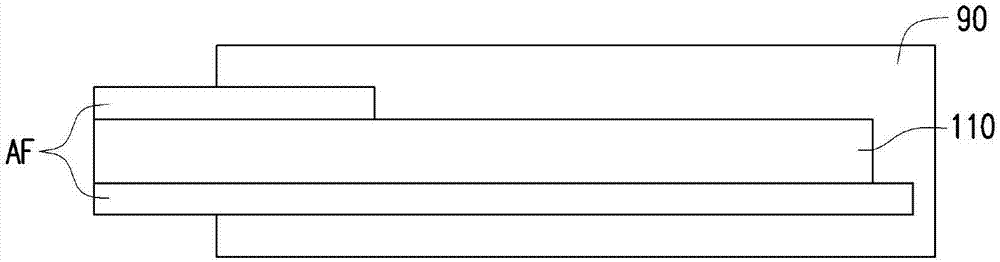
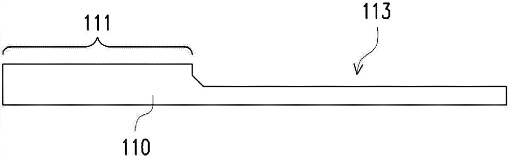
[0039] Figures 1A to 1F It is a schematic flowchart of the manufacturing method of the touch panel according to the first embodiment of the present invention. Figures 1A to 1F The cross-sectional structure diagrams of the touch panels are respectively shown. Figure 1G Yes Figure 1F Front view of the touch panel. First, a substrate 110 is provided, wherein the substrate 110 has a first surface S111 and a second surface S112 opposite to each other. In this embodiment, the substrate 110 is, for example, a glass substrate, but the invention is not limited thereto. In other embodiments, the material of the substrate 110 may be other light-transmitting materials. In addition, in this embodiment, the maximum thickness of the substrate 110 ranges from 700 μm to 1000 μm. It should be noted that the above-mentioned parameter ranges are only illustrative, and are not intended to limit the present invention. The thickness of the substrate 110 can be determined according to the des...


PUM


Abstract

The invention provides a touch panel and a manufacturing method thereof. The touch panel is used for providing a touch signal. The touch panel comprises a substrate, a first vision shielding layer, an electrode layer and a metal material layer. The substrate is provides with a display region and a first groove part. The first vision shielding layer is partially or completely embedded in the first groove part. One part of the electrode layer is arranged on the display region, while the other part of the electrode layer is arranged on the first vision shielding layer. When an object touches with or is close to the touch panel, the electrode layer correspondingly generates a touch signal. The metal material layer is arranged on the first vision shielding layer and is electrically connected with the electrode layer to transfer the touch signal to a drive element.

Description

technical field [0001] The present invention relates to a touch electronic device, in particular to a touch panel and a manufacturing method thereof. Background technique [0002] In recent years, with the increasing development of the technology industry, electronic devices such as notebook computers (Notebook, NB), tablet computers (Tablet PC) and smart phones (Smart Phone) have frequently appeared in daily life. Among them, some electronic devices have the characteristics of being light, thin, and short, so that users can operate them by hand and are convenient to carry. The forms and functions of electronic devices are becoming more and more diverse, and the convenience and practicality make these electronic devices more popular and can be used for different purposes. Therefore, the user can hold the electronic device with one hand, and operate the electronic device by touching or pressing the keyboard or the touch panel located on the operation surface of the electroni...

Claims


Application Information

Patent Timeline
Patent Type & Authority Patents(China)
IPC IPC(8): G06F3/041
CPCG06F3/0412G06F2203/04103
Inventor 郭峻廷陈志强
Owner ACER INC
Why Eureka
Try Eureka