A method of manufacturing a touch screen protection substrate realizing an ultra-narrow bezel
A technology for protecting a substrate and a manufacturing method, which is applied to the manufacturing field of a protective substrate for a touch screen, can solve problems such as affecting the appearance of a handheld electronic device, a small display area of a display, etc., and achieves the saving of test work, the best narrow frame effect, and the effect of reducing the frame.
- Summary
- Abstract
- Description
- Claims
- Application Information
AI Technical Summary
Problems solved by technology
Method used
Image
Examples
Embodiment 1
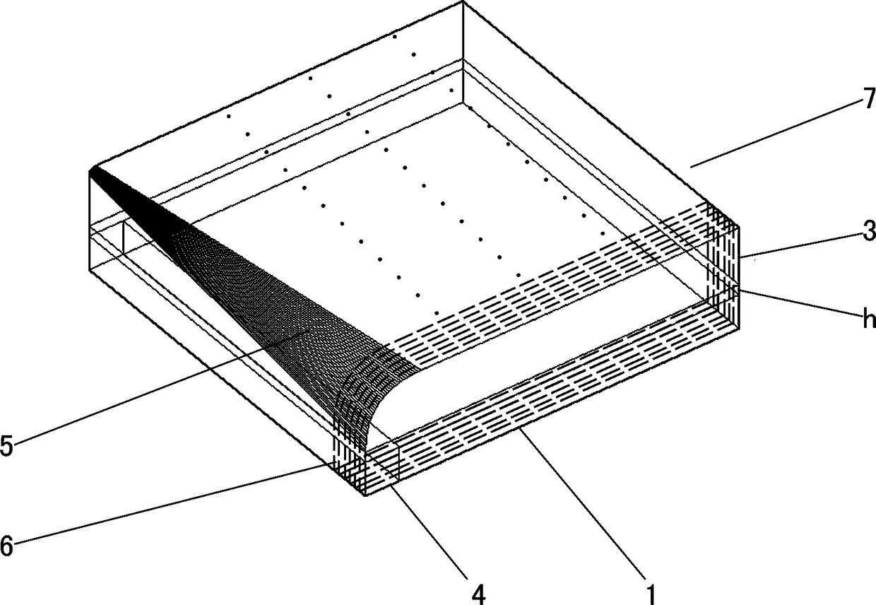
[0032] like figure 1 As shown, the manufacturing method of the touch screen protective substrate realizing the ultra-narrow frame includes the following steps:
[0033] (1), establish a plurality of different 3D models, each 3D model includes a simulated background color layer 1 and a simulated transparent substrate 3 having a refractive index and thickness arranged on the simulated background color layer 1, and the simulated background color layer 1 is provided with The edge black frame 4 simulates that the transparent substrate 3 has an edge chamfer 5, and the edge chamfer 5 corresponds to the position of the edge black frame 4; each 3D model is the same except that the edge chamfer 5 is inconsistent; then make each The edge chamfer 5 in the 3D model changes gradually, and then slices 6 with the edge chamfer 5 are cut from each 3D model, and each slice 6 with the edge chamfer 5 is superimposed on the Together form a laminated 3D model 7, the edge chamfer 5 adopts a positive...
Embodiment 2
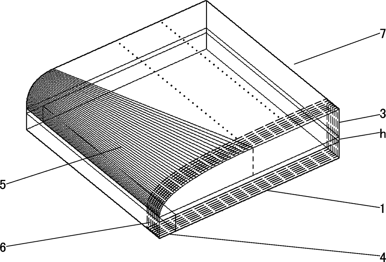
[0039] Under the situation that other parts are all identical with embodiment one, its difference is: as image 3 As shown, in step (1), the edge chamfer 5 of each slice 6 is an elliptical arc chamfer, and the ratio of the longitudinal axis to the transverse axis of the ellipse gradually changes according to the order of the overlapping of each slice 6, wherein the semi-short axis of the ellipse is 1.7mm, the semi-major axis > 1.7mm, the elliptical arc gradually changes; in step (2), the widest part C of the screen overflows is the best narrow frame effect, and the semi-major axis of the ellipse arc corresponding to the best point is 2.3mm, semi-short The axis is 1.7mm, and the corresponding optimal ellipse arc chamfer is as follows Figure 4as shown in D; Figure 5 As shown, in step (3), select the slice 6 corresponding to the position E where the narrow border effect is the best, and rebuild the optimal 3D model according to the edge chamfer 5 of the slice 6 .
Embodiment 3
[0041] In the case that other parts are the same as in the second embodiment, the difference is that the thickness of the simulated transparent substrate 3 is reduced to 1.0 mm, and the semi-minor axis is 0.7 mm.
[0042] like Image 6 , Figure 7 , Figure 8 As shown by F, G, and H in the figure, as the semi-major axis of the ellipse arc increases, the overflowing part F of the picture first increases and then decreases. The semi-major axis of G is 2.7mm, the semi-minor axis is 0.7mm, and the part F of the screen overflows is less, and the overall effect is not obvious.
PUM
 Abstract
Description
Claims
Application Information


