Supercharge Your Innovation With Domain-Expert AI Agents!

A kind of preparation method of array substrate

An array substrate and process technology, which is applied in the field of array substrate preparation, can solve problems such as the complexity of the array substrate preparation process, and achieve the effects of improving the yield rate of manufactured products, reducing costs, and reducing complexity

Active Publication Date: 2017-09-22
TCL CHINA STAR OPTOELECTRONICS TECH CO LTD
View PDF3 Cites 0 Cited by
  • Summary
  • Abstract
  • Description
  • Claims
  • Application Information

AI Technical Summary

Problems solved by technology

[0004] The purpose of the present invention is to provide a method for preparing an array substrate, so as to solve the technical problem that the preparation process of the array substrate is complicated in the touch screen adopting in-cell technology

Method used


Image

  • A kind of preparation method of array substrate
  • A kind of preparation method of array substrate
  • A kind of preparation method of array substrate

Examples


Embodiment Construction

[0041] The implementation of the present invention will be described in detail below in conjunction with the accompanying drawings and examples, so as to fully understand and implement the process of how to apply technical means to solve technical problems and achieve technical effects in the present invention. It should be noted that, as long as there is no conflict, each embodiment and each feature in each embodiment of the present invention can be combined with each other, and the formed technical solutions are all within the protection scope of the present invention.

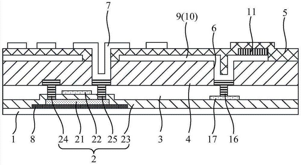
[0042] An embodiment of the present invention provides a method for preparing an array substrate. Such as figure 1 As shown, the array substrate includes a plurality of pixel units, and each pixel unit is provided with a thin film transistor 2 and a pixel electrode 7 . The TFT 2 in the embodiment of the present invention is a top-gate TFT using Low Temperature Poly-Silicon (LTPS for short). In the thin fil...


PUM


Abstract

The invention discloses a method for preparing an array substrate, which belongs to the field of display technology, and aims to solve the technical problem that the preparation process of the array substrate is complicated in a touch screen adopting in-cell technology. The preparation method of the array substrate includes: sequentially forming a transparent conductive film and a metal film; using a photomask process, forming the transparent conductive film into an address electrode, and simultaneously forming the metal film into a metal structure that matches the address electrode , the mask process is a half-tone mask process or a gray tone mask process. The invention can be used in electronic devices such as mobile phones and tablet computers.

Description

technical field [0001] The present invention relates to the field of display technology, in particular to a method for preparing an array substrate. Background technique [0002] With the popularity of smart electronic products, capacitive touch screens are widely used in various electronic products such as mobile phones and tablet computers. At present, the more common capacitive touch screens include OGS (One Glass Solution), on-cell and in-cell technologies. Among them, due to its advantages in manufacturing process, in-cell technology has the advantages of lighter and thinner, better light transmission and more stable structure compared with OGS technology and on-cell technology. [0003] The inventors have found that in order to reduce the resistance of the address electrodes, a metal structure needs to be matched with the address electrodes in the touch screen adopting the in-cell technology. However, the appearance of the metal structure will increase the complexity...

Claims


Application Information

Patent Timeline
Patent Type & Authority Patents(China)
IPC IPC(8): G06F3/041G06F3/044
CPCG06F3/044G06F2203/04103G02F1/1362G06F3/041H01L21/77G06F3/0443
Inventor 薛景峰陈归
Owner TCL CHINA STAR OPTOELECTRONICS TECH CO LTD
Features
  • R&D
  • Intellectual Property
  • Life Sciences
  • Materials
  • Tech Scout
  • Unparalleled Data Quality
  • Higher Quality Content
  • 60% Fewer Hallucinations
Learn More