Printed circuit board for optical module

A printed circuit board and circuit board technology, applied in the direction of printed circuits connected to non-printed electrical components, can solve the problems of signal integrity deterioration, signal crosstalk, etc., to reduce the height and number, eliminate signal crosstalk, Eliminate the effect of vias

Active Publication Date: 2015-04-22
旭创科技有限公司
View PDF3 Cites 3 Cited by
  • Summary
  • Abstract
  • Description
  • Claims
  • Application Information

AI Technical Summary

Problems solved by technology

[0003] The above disadvantages of the printed circuit board in the prior art are: first, since the data transmission path at the transmitting end and the data transmission path at the receiving end are arranged on the same surface of the printed circuit board, the data transmission path at the transmitting end and the data transmission path at the receiving end are arranged on the same surface of the printed circuit board. There is a phenomenon of signal crosstalk between the data transmission paths at the receiving end; second, because the optical component interface at the transmitting end and the component interface at the receiving end are arranged on one surface of the printed circuit board, and the data interface at the transmitting end and the receiving end data interface are arranged on the printed circuit board. On both surfaces of the circuit board, so when forming the data transmission path at the transmitting end and the data transmission path at the receiving end, some circuit board wiring needs to be connected to the printed circuit board through one or more vias from one surface of the printed circuit board. another surface, resulting in poor signal integrity

Method used


Image

  • Printed circuit board for optical module
  • Printed circuit board for optical module
  • Printed circuit board for optical module

Examples


Embodiment Construction

[0022] In order to better understand and explain the present invention, the present invention will be further described in detail below with reference to the accompanying drawings.

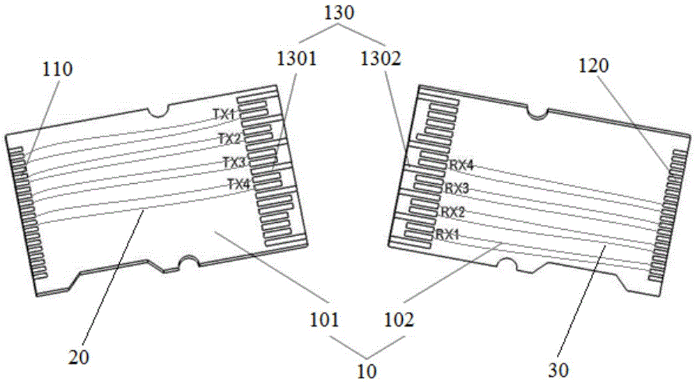
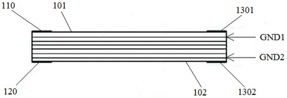
[0023] The present invention provides a printed circuit board for an optical module. Please refer to figure 2 and image 3 ,in, figure 2 is a schematic diagram of the structure of the first surface and the second surface of the printed circuit board according to the present invention, image 3 Yes figure 2 A schematic cross-sectional view of the printed circuit board shown. As shown in the figure, the printed circuit board includes a substrate 10, an optical component interface 110 at the transmitting end, an optical component interface 120 at the receiving end, an electrical interface 130, a first circuit board connection 20, and a second circuit board connection 30. The The electrical interface 130 includes a transmitter data interface 1301 and a receiver data interface 1302, wherein:

...


PUM


Abstract

The invention provides a printed circuit board for an optical module. The printed circuit board for the optical module comprises a base plate, transmitting terminal light component interfaces, receiving terminal light component interfaces, electrical interfaces, first circuit board wiring and second circuit board wiring; the electrical interfaces comprise transmitting terminal data interfaces and receiving terminal data interfaces, the base plate comprises a first surface and a second surface opposite to the first surface, the transmitting terminal light component interfaces and the transmitting terminal data interfaces are arranged on the first surface and connected with each other through the first circuit board wiring to form a transmitting terminal data transmission path, and the receiving terminal light component interfaces and the receiving terminal data interfaces are arranged on the second surface and connected with each other through the second circuit board wiring to form a receiving terminal data transmission path. By means of the printed circuit board for the optical module, the signal crosstalk between the transmitting terminal data transmission path and the receiving terminal data transmission path can be effectively reduced or even basically eliminated, and the integrity of the signals can be greatly improved.

Description

technical field [0001] The invention relates to the field of electronic components, in particular to a printed circuit board for an optical module. Background technique [0002] The printed circuit board is one of the important components of the optical module. Typically, the printed circuit board includes a substrate, a transmitting-end optical component interface, a receiving-end optical component interface, and an electrical interface, wherein the electrical interface further includes a transmitting-end data interface and a receiving-end data interface. The transmitting end optical component interface and the receiving end optical component interface of the printed circuit board are arranged on one surface of the substrate, wherein the transmitting end optical component interface is used for connecting with the transmitting end optical component in the optical module, and the receiving end optical component interface is used for Connect to the receiving end optical compo...

Claims


Application Information

Patent Timeline
Patent Type & Authority Applications(China)
IPC IPC(8): H05K1/18
Inventor 王祥忠孙雨舟王克武徐晓明
Owner 旭创科技有限公司
Why Eureka
Try Eureka