Supercharge Your Innovation With Domain-Expert AI Agents!

Determining method of via hole parameter and via hole impedance value on circuit board

A technology to determine the method and impedance value, which is applied in the direction of measuring resistance/reactance/impedance, electronic circuit testing, measuring electrical variables, etc., and can solve problems such as high cost, long development cycle, and inability to quantitatively analyze circuit boards.

Active Publication Date: 2015-05-06
NEW FOUNDER HLDG DEV LLC +2
View PDF6 Cites 10 Cited by
  • Summary
  • Abstract
  • Description
  • Claims
  • Application Information

AI Technical Summary

Problems solved by technology

[0005] Embodiments of the present invention provide a method for determining via hole parameters and via impedance values ​​on a circuit board, so as to solve the problem that the influence of via design on the circuit board cannot be quantitatively analyzed at present. When a problem is found in the circuit board design test, it needs Multiple revisions can solve the problem, the development cycle is long, and the cost is high

Method used


Image

  • Determining method of via hole parameter and via hole impedance value on circuit board
  • Determining method of via hole parameter and via hole impedance value on circuit board
  • Determining method of via hole parameter and via hole impedance value on circuit board

Examples


Embodiment Construction

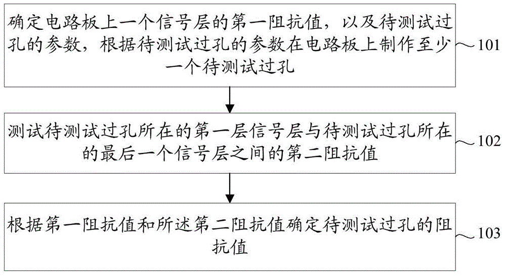
[0041] The embodiment of the present invention provides a method for determining via hole parameters and via hole impedance values ​​on a circuit board, determining via hole impedance values ​​corresponding to different via hole parameters, and quantitatively analyzing the influence of parameters on via hole impedance values According to the impedance value of the required circuit, determine the parameters of the via hole whose impedance value meets the impedance value of the required circuit, reduce the number of circuit design revisions caused by the impedance value of the via hole, shorten the development cycle, and reduce costs.

[0042] Embodiments of the present invention will be further described below in conjunction with the accompanying drawings.

[0043] Such as figure 1 As shown, it is a method for determining the impedance value of a via on a circuit board in an embodiment of the present invention. The method includes:

[0044] Step 101: Determine the first impeda...


PUM


Abstract

The invention relates to the field of manufacturing semiconductor, and specifically relates to a determining method of via hole parameter and via hole impedance value on circuit board, so as to solve the problem that the affection of via hole design to the circuit board cannot be quantitatively analyzed; when a problem is found in testing the circuit board design, several large corrections are required to solve the problem; the development period is long; and the cost is very high. By obtaining the correspondence between the parameter of the via hole to be tested and the impedance value of the via hole to be tested, the embodiments of the invention quantitatively analyze the affection of the parameter of the via hole to be tested to the impedance value of the via hole to be tested, and determine the via hole parameter satisfying the require circuit board impedance value based on the correspondence between the parameter of the via hole to be tested and the impedance value of the via hole to be tested, thereby shortening the development period, reducing the number of large corrections caused by the unreasonable design of the via hole, and reducing the cost.

Description

technical field [0001] The invention relates to the field of semiconductor manufacturing, in particular to a method for determining via hole parameters and via hole impedance values ​​on a circuit board. Background technique [0002] With the development of digital signal processing theory and the emergence of digital circuits, digital circuits are widely used to realize various functions. In digital products, the binary code stream composed of "0" and "1" is used to transmit information, and the binary code "0" and "1" are represented by high and low levels, which greatly improves the anti-noise performance of the product. However, with the continuous improvement of circuit operating frequency, whether the code stream of "0" and "1" can be accurately transmitted to the receiving end, and whether the receiving end can accurately judge it has become a new problem. [0003] The "0" and "1" codes are transmitted through voltage or current waveforms. Although the information is...

Claims


Application Information

Patent Timeline
IPC IPC(8): G01R27/02G01R31/28
Inventor 余凯胡新星刘丰
Owner NEW FOUNDER HLDG DEV LLC
Features
  • R&D
  • Intellectual Property
  • Life Sciences
  • Materials
  • Tech Scout
  • Unparalleled Data Quality
  • Higher Quality Content
  • 60% Fewer Hallucinations
Learn More