Packaging process for new fingerprint lock devices

A packaging technology and fingerprint lock technology, which is applied in semiconductor/solid-state device manufacturing, electrical components, circuits, etc., can solve the problems of reducing the height of the module, improve product reliability, simplify the manufacturing process, improve the stability of wire connection and reliability effect

Active Publication Date: 2017-10-13
苏州科阳半导体有限公司
View PDF8 Cites 0 Cited by
  • Summary
  • Abstract
  • Description
  • Claims
  • Application Information

AI Technical Summary

Problems solved by technology

The Touch ID packaging structure announced by Apple’s patent text is realized by wire bonding, but only grooves are dug on the surface of the chip to reduce the height of the module after wire bonding. I have not seen the packaging form and patent of the fingerprint identification chip that really adopts the wafer-level TSV packaging technology

Method used


Image

  • Packaging process for new fingerprint lock devices
  • Packaging process for new fingerprint lock devices
  • Packaging process for new fingerprint lock devices

Examples


Embodiment 1

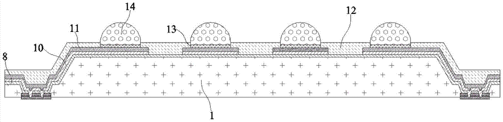
[0037] Embodiment 1: a kind of packaging technology for novel fingerprint lock device, described novel fingerprint lock device comprises fingerprint identification chip 1, ceramic cover plate 15, flexible PCB board 16 and data processing chip 17, the fingerprint identification chip 1 A high dielectric constant layer 18 is arranged between the sensing area and the ceramic cover plate 15, and the flexible PCB board 16 and the data processing chip 17 are electrically connected to the fingerprint recognition chip 1;

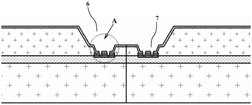
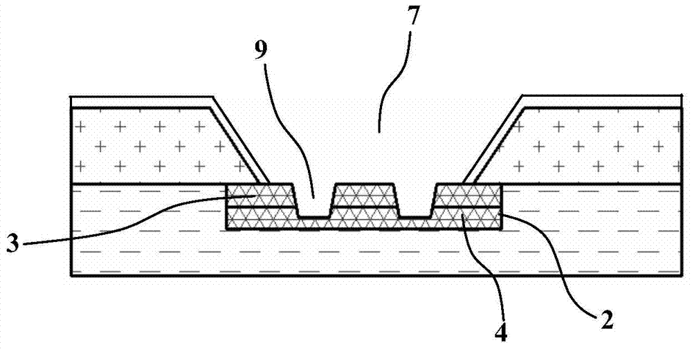
[0038] Several blind holes 2 are distributed on the upper surface of the fingerprint identification chip 1, and the blind holes 2 of the fingerprint identification chip 1 have an aluminum pad 3, and the aluminum pad 3 extends from the bottom of the blind hole 2 to the middle of the blind hole 2, and The surface of the aluminum pad 3 in the hole 2 is filled with a nickel metal layer 4, and the nickel metal layer 4 extends from the middle of the blind hole 2 to the uppe...

Embodiment 2

[0052] Embodiment 2: A kind of packaging technology for novel fingerprint lock device, described novel fingerprint lock device comprises fingerprint identification chip 1, ceramic cover plate 15, flexible PCB board 16 and data processing chip 17, the fingerprint identification chip 1 A high dielectric constant layer 18 is arranged between the sensing area and the ceramic cover plate 15, and the flexible PCB board 16 and the data processing chip 17 are electrically connected to the fingerprint recognition chip 1;

[0053] Several blind holes 2 are distributed on the upper surface of the fingerprint identification chip 1, and the blind holes 2 of the fingerprint identification chip 1 have an aluminum pad 3, and the aluminum pad 3 extends from the bottom of the blind hole 2 to the middle of the blind hole 2, and The surface of the aluminum pad 3 in the hole 2 is filled with a nickel metal layer 4, and the nickel metal layer 4 extends from the middle of the blind hole 2 to the uppe...


PUM


Abstract

The invention discloses a packaging process for a novel fingerprint lock device, including a fingerprint identification chip, a ceramic cover plate, a flexible PCB board and a data processing chip, and a nickel metal layer is filled on the surface of an aluminum pad in a blind hole of the fingerprint identification chip, thereby The upper surface is raised and formed to form a pad thickening part; a temporary bonding adhesive layer is applied on the upper surface of the fingerprint recognition chip with a pad thickening part; a glass support plate is passed through the temporary bonding adhesive layer and the fingerprint The identification chip has the upper surface of the thickened part of the pad bonded; the lower surface opposite to the upper surface of the fingerprint identification chip is thinned, thereby reducing the thickness of the fingerprint identification chip to about 150-300 microns; from the lower surface of the fingerprint identification chip The first tapered blind hole, the second tapered blind hole and the third tapered blind hole are sequentially realized by stepwise etching. The invention integrates wafer-level chip packaging and through-silicon via technology to form a new set of process flow, reduces thickness, greatly reduces the total thickness of the product, and greatly improves product reliability.

Description

technical field [0001] The invention relates to a packaging process for a novel fingerprint lock device, which belongs to the technical field of semiconductor packaging. Background technique [0002] In terms of advanced packaging technology for fingerprint chips, after the release of Apple's iPhone 5S and its matching TouchID fingerprint recognition technology, it announced a brand new fingerprint recognition chip. It uses wafer-level packaging technology to dig grooves on the side of each chip and redo the pads, and then uses the well-known low loop height (low loop height) wire bonding technology to complete the module packaging to reduce the number of modules. High, is a transitional technology that mixes wafer-level packaging and traditional packaging. The Touch ID packaging structure announced by Apple’s patent text is realized by wire bonding, but only grooves are dug on the surface of the chip to reduce the height of the module after wire bonding. We have not seen ...

Claims


Application Information

Patent Timeline
Patent Type & Authority Patents(China)
IPC IPC(8): H01L21/50H01L21/60
Inventor 黄双武赖芳奇王邦旭吕军刘辰
Owner 苏州科阳半导体有限公司
Why Eureka
Try Eureka