Manufacturing method of light-emitting device with crystal coated light emitting diode

A technology of light-emitting diodes and light-emitting devices, which is applied in semiconductor/solid-state device manufacturing, semiconductor devices, electrical components, etc., and can solve problems such as lower yield rate and cumbersome manufacturing process

Inactive Publication Date: 2007-12-05
NEOBULB TECHNOLOGIES INC
View PDF4 Cites 0 Cited by
  • Summary
  • Abstract
  • Description
  • Claims
  • Application Information

AI Technical Summary

Problems solved by technology

[0004] However, the above-mentioned light-emitting core body 1 needs to go through the steps of die bonding and wire bonding of the substrate before the wiring of the light-emitting diode 10 can be guided to the electrodes 16 and 18 on both sides, so the manufacturing process is comparatively relatively short. It is cumbersome, and there is an additional wire bonding process, which still cannot avoid damage to the light-emitting diode 10 and the substrate 12 during the manufacturing process, thereby reducing the yield

Method used


Image

  • Manufacturing method of light-emitting device with crystal coated light emitting diode
  • Manufacturing method of light-emitting device with crystal coated light emitting diode
  • Manufacturing method of light-emitting device with crystal coated light emitting diode

Examples


Embodiment Construction

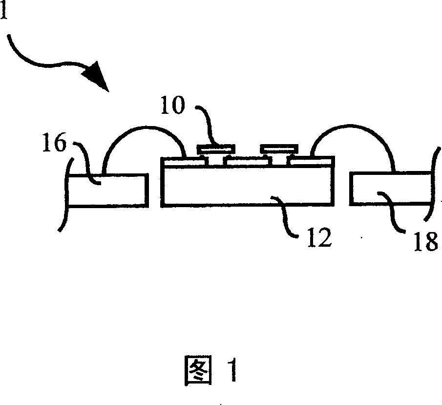
[0021] Aiming at the problems of cumbersome manufacturing process, poor yield rate and poor heat dissipation caused by the luminous body in the prior art, the present invention proposes a manufacturing method of a light-emitting device with flip-chip light-emitting diodes.

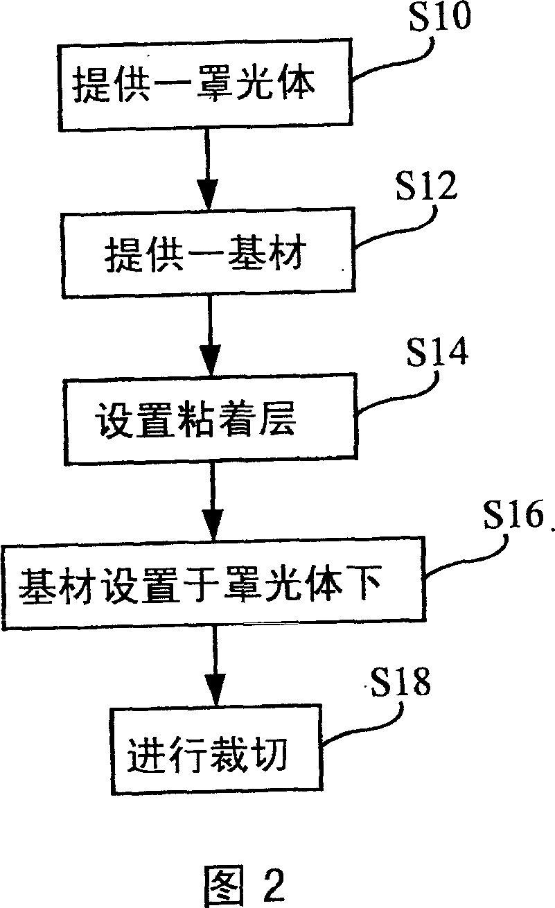
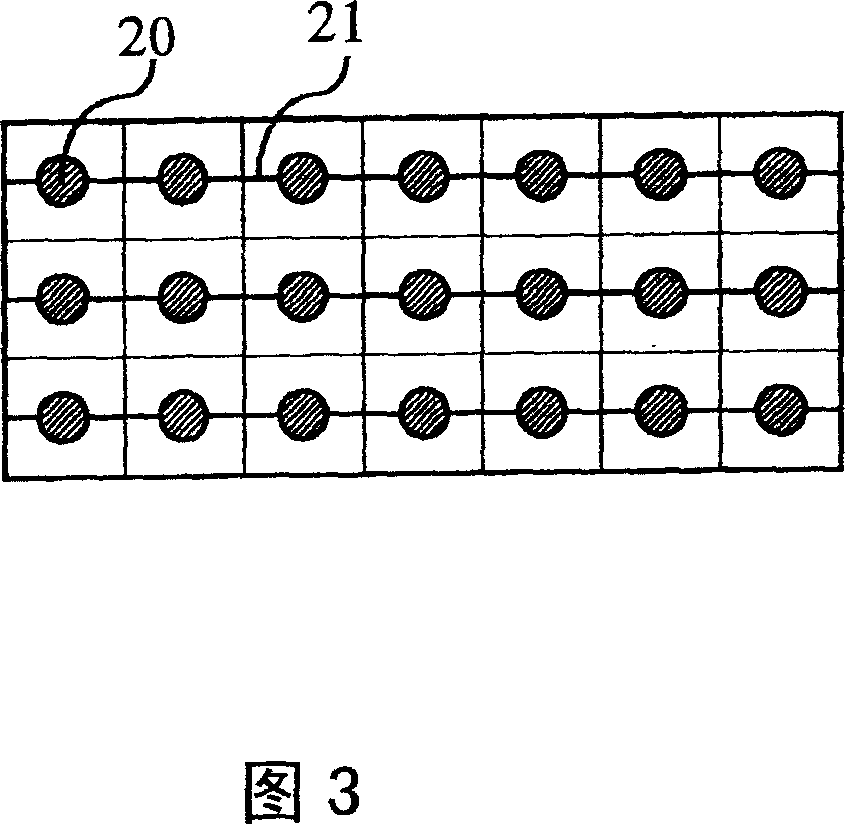
[0022] Fig. 2 shows the flow chart of manufacturing the light-emitting device with flip-chip light-emitting diodes of the present invention. At first, as step S10, a masking body group (strap) is provided, and please refer to the schematic diagram shown in Fig. 3 at the same time, the masking body The group includes several light-shielding bodies 20, and a metal lead frame 21 is arranged in each light-shielding body 20, and each two light-shielding bodies 20 are connected to each other through the metal lead frame 21, and then as in step S12, a base material, such as a silicon (Si) substrate, on which several light-emitting diodes are arranged as light-emitting elements, and these light-emitting diodes are ...


PUM


Abstract

The present invention proposes the making process of composite crystal LED. The making process includes the steps of: providing several light housing with metal wire frame, providing one substrate with composite crystal LED under the light housing, fixing the substrate under the light housing with one metal connecting layer and connecting the substrate electrically with the metal wire frame inside the light housing, and cutting in light housing as unit to form several light emitter with composite crystal LED. The present invention can simplifies the making process, and has high efficiency and product quality and heat radiating efficiency.

Description

technical field [0001] The invention relates to a manufacturing method of a light-emitting device, in particular to a manufacturing method of a light-emitting device with flip-chip light-emitting diodes that can simplify the manufacturing process. Background technique [0002] Lighting devices have become an indispensable consumable in today's human life. In response to different application requirements, many lighting devices have been continuously developed and improved to facilitate people's lives. [0003] FIG. 1 is a cross-sectional view of the current electrical connection structure of flip-chip light-emitting diodes applied to lighting modules. The light-emitting core body 1 is provided with flip-chip light-emitting diodes 10 on a substrate 12. These flip-chip light-emitting diodes 10 It is necessary to guide the circuit to the electrodes 16 and 18 on both sides by wire bonding on the substrate, so as to facilitate the operation of the light emitting diode 10 by exter...

Claims


Application Information

Patent Timeline
Patent Type & Authority Patents(China)
IPC IPC(8): H01L33/00H01L25/075H01L21/50
CPCH01L2224/48091H01L2924/00014
Inventor 陈振贤林俊仁
Owner NEOBULB TECHNOLOGIES INC
Why Eureka
Try Eureka