Fingerprint lock chip manufacturing technology

A manufacturing process and fingerprint lock technology, applied in the field of fingerprint lock chip manufacturing process, can solve the problems of reducing the height of the module, not seeing the fingerprint lock chip, etc., to improve product reliability, high-efficiency integrated fingerprint recognition, small volume effect

Active Publication Date: 2015-06-03
苏州科阳半导体有限公司
View PDF3 Cites 0 Cited by
  • Summary
  • Abstract
  • Description
  • Claims
  • Application Information

AI Technical Summary

Problems solved by technology

The Touch ID packaging structure announced by Apple’s patent text is realized by wire bonding, but only grooves are dug on the surface of the chip to reduce the height of the module after wire bonding. No fingerprint lock chip packaging form and patents that actually use wafer-level TSV packaging technology have been seen

Method used


Image

  • Fingerprint lock chip manufacturing technology
  • Fingerprint lock chip manufacturing technology
  • Fingerprint lock chip manufacturing technology

Examples


Embodiment 1

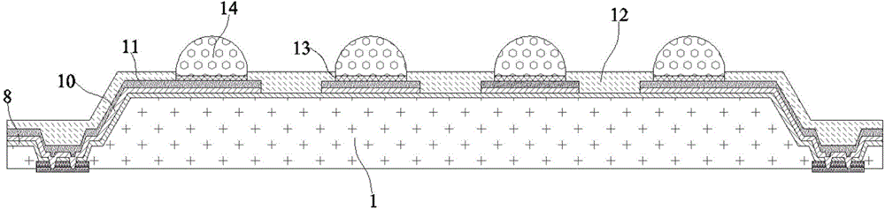
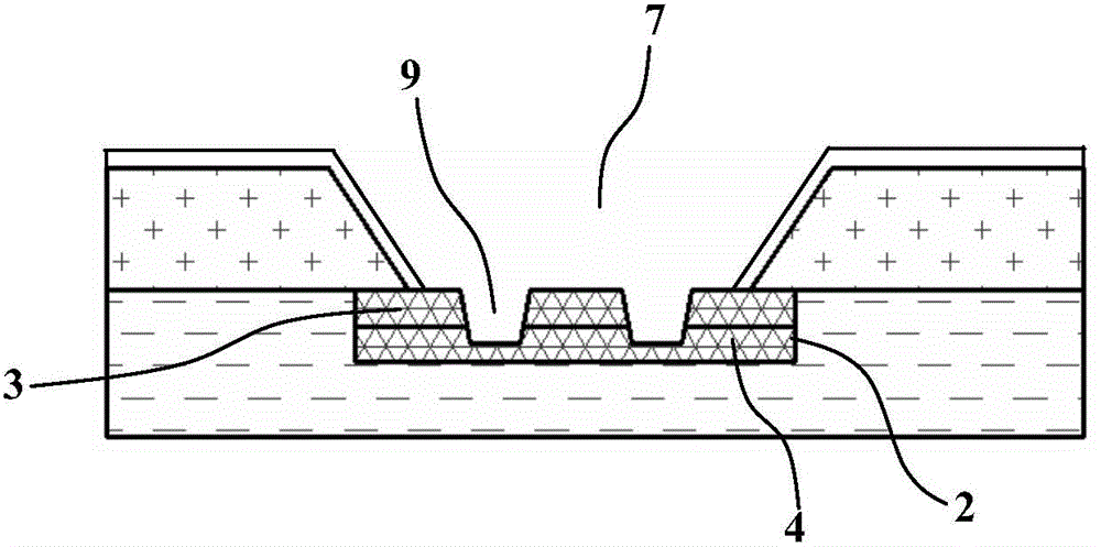
[0033] Embodiment 1: A manufacturing process of a fingerprint lock chip, the upper surface of the fingerprint lock chip 1 is distributed with several blind holes 2, and there is an aluminum pad 3 in the blind hole 2 of the fingerprint lock chip 1, the aluminum pad 3 extends from the bottom of the blind hole 2 to the middle of the blind hole 2, the surface of the aluminum pad 3 in the blind hole 2 is filled with a nickel metal layer 4, and the nickel metal layer 4 extends from the middle of the blind hole 2 to the upper surface of the fingerprint lock chip 1 and forms a convex to form a pad thickening part 5;

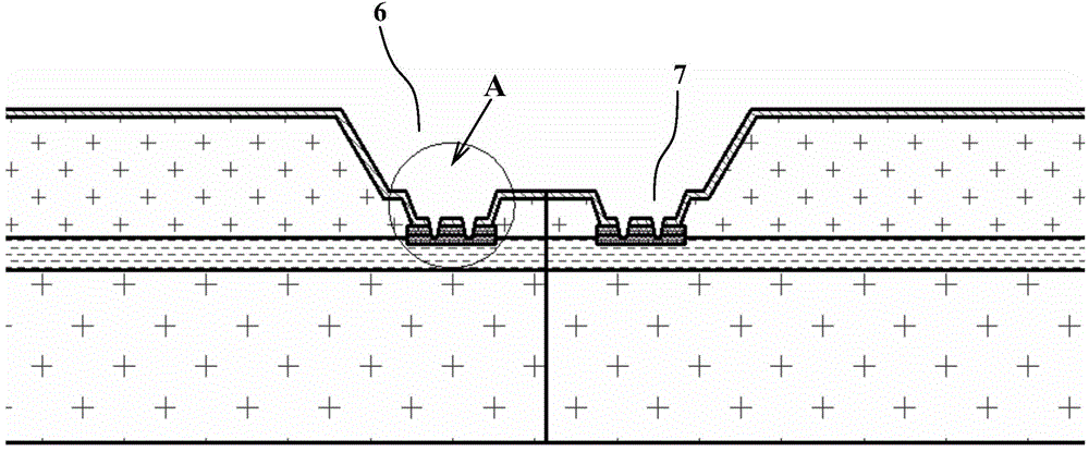
[0034] The lower surface of the fingerprint lock chip 1 and the area opposite to the blind hole 2 have a first tapered blind hole 6 and a second tapered blind hole 7 from outside to inside, and the second tapered blind hole 7 is located in the first tapered blind hole. At the bottom of the hole 6, the cross section of the first tapered blind hole 6 and the second tapered...

Embodiment 2

[0045] Embodiment 2: A manufacturing process of a fingerprint lock chip, the upper surface of the fingerprint lock chip 1 is distributed with several blind holes 2, and there is an aluminum pad 3 in the blind hole 2 of the fingerprint lock chip 1, the aluminum pad 3 extends from the bottom of the blind hole 2 to the middle of the blind hole 2, the surface of the aluminum pad 3 in the blind hole 2 is filled with a nickel metal layer 4, and the nickel metal layer 4 extends from the middle of the blind hole 2 to the upper surface of the fingerprint lock chip 1 and forms a convex to form a pad thickening part 5;

[0046] The lower surface of the fingerprint lock chip 1 and the area opposite to the blind hole 2 have a first tapered blind hole 6 and a second tapered blind hole 7 from outside to inside, and the second tapered blind hole 7 is located in the first tapered blind hole. At the bottom of the hole 6, the cross section of the first tapered blind hole 6 and the second tapered...


PUM


Abstract

The invention discloses a fingerprint lock chip manufacturing technology. The fingerprint lock chip manufacturing technology comprises the following steps: filling nickel metal layers on the surfaces of aluminum welding pads in blind holes of a fingerprint lock chip to form bonding pad thickening parts; forming insulating layers on the surfaces of a first tapered blind hole and a second tapered blind hole in the lower surface of the fingerprint lock chip; forming a plurality of third tapered blind holes in the bottom of the second tapered blind hole; sequentially forming titanium metal conductive pattern layers and copper metal conductive pattern layers above the tapered blind holes; coating the upper surface, having the bonding pad thickening parts, of the fingerprint lock chip with a temporary bonding adhesive layer; bonding a glass supporting plate with the surface, having the bonding pad thickening parts, of the fingerprint lock chip through the temporary bonding adhesive layer; thinning the lower surface opposite to the upper surface of the fingerprint lock chip. After wafer-level chip packaging technology and a silicon through hole technology are integrated, a novel process flow is formed, so that the thickness is reduced and the total thickness of a product is greatly reduced; by the manufacturing technology, a 0.4mm solid can exist in a 0.5mm packaging body, so that the reliability of the product is greatly improved.

Description

technical field [0001] The invention relates to a manufacturing process of a fingerprint lock chip, belonging to the technical field of semiconductor packaging. Background technique [0002] In terms of advanced packaging technology for fingerprint chips, after the release of Apple's iPhone 5S and its matching Touch ID fingerprint recognition technology, it announced a brand new fingerprint recognition technology. After the release, it announced a brand new fingerprint lock chip , which uses the wafer-level packaging technology to dig grooves on the side of each chip and redo the pads, and then uses the well-known low loop height (low loop height) wire bonding technology to complete the module packaging in the later stage to reduce the mold Group height is a transitional technology that mixes wafer-level packaging and traditional packaging. The Touch ID packaging structure announced by Apple’s patent text is realized by wire bonding, but only grooves are dug on the surface ...

Claims


Application Information

Patent Timeline
Patent Type & Authority Applications(China)
IPC IPC(8): H01L21/768
CPCH01L21/76838H01L21/76877H01L21/76895H01L2221/1068
Inventor 黄双武赖芳奇王邦旭吕军刘辰
Owner 苏州科阳半导体有限公司
Why Eureka
Try Eureka