Fingerprint lock identification module package structure

A technology of fingerprint identification and packaging structure, which is applied in the direction of character and pattern recognition, instruments, electrical components, etc., can solve the problems of reducing the height of modules, improve product reliability, enhance data processing speed and electrical stability, and manufacture The effect of simple process

Active Publication Date: 2018-07-13
苏州科阳半导体有限公司
View PDF5 Cites 0 Cited by
  • Summary
  • Abstract
  • Description
  • Claims
  • Application Information

AI Technical Summary

Problems solved by technology

The Touch ID packaging structure announced by Apple’s patent text is realized by wire bonding, but only grooves are dug on the surface of the chip to reduce the height of the module after wire bonding. I have not seen the packaging form and patent of the fingerprint identification chip that really adopts the wafer-level TSV packaging technology

Method used


Image

  • Fingerprint lock identification module package structure
  • Fingerprint lock identification module package structure
  • Fingerprint lock identification module package structure

Examples


Embodiment 1

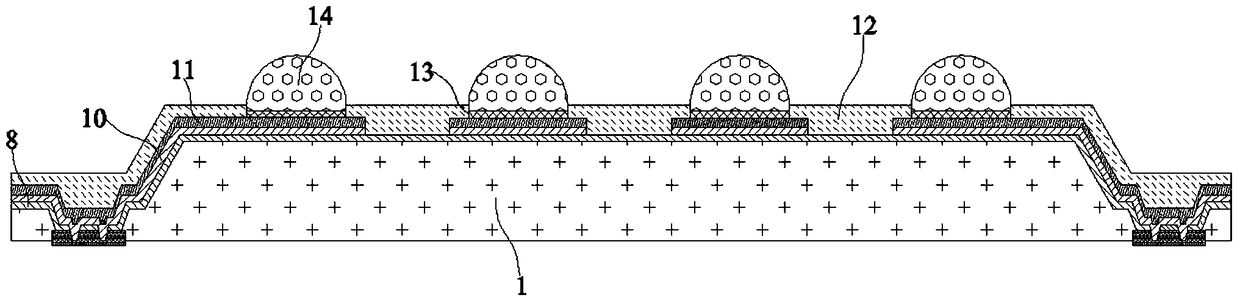
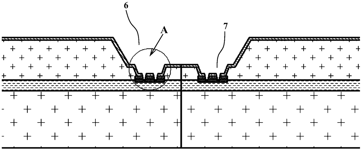
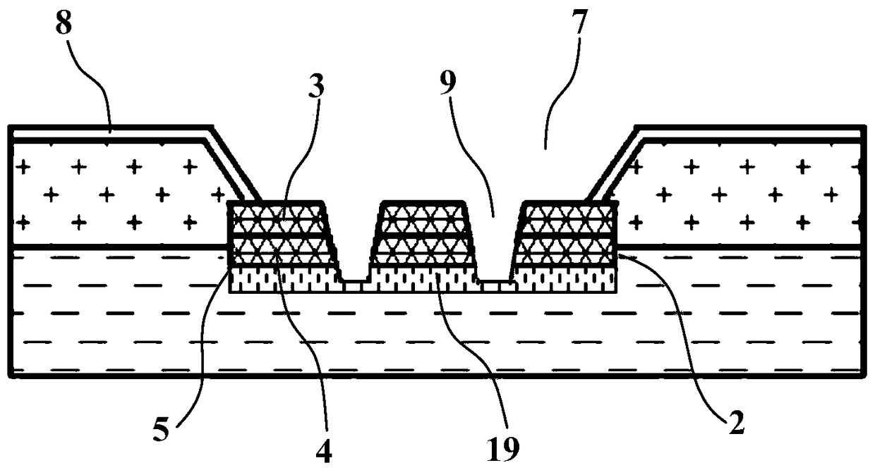
[0026] Embodiment 1: A fingerprint lock identification module packaging structure, including a fingerprint identification chip 1, a ceramic cover plate 15, a PCB board 16 and a data processing chip 17, between the sensing area of ​​the fingerprint identification chip 1 and the ceramic cover plate 15 A high dielectric constant layer 18 is provided, and the PCB board 16 and the data processing chip 17 are electrically connected to the fingerprint identification chip 1;

[0027] There are several blind holes 2 distributed on the upper surface of the fingerprint recognition chip 1, and the blind holes 2 of the fingerprint recognition chip 1 have an aluminum pad 3, and the aluminum pad 3 extends from the bottom of the blind hole 2 to the middle of the blind hole 2, The surface of aluminum pad 3 in blind hole 2 is covered with nickel metal layer 4 and gold-palladium alloy layer 19 in turn. The thick part 5, the gold-palladium alloy layer 19 is located on the surface of the pad thick...

Embodiment 2

[0031] Embodiment 2: A fingerprint lock identification module packaging structure, including a fingerprint identification chip 1, a ceramic cover plate 15, a PCB board 16 and a data processing chip 17, between the sensing area of ​​the fingerprint identification chip 1 and the ceramic cover plate 15 A high dielectric constant layer 18 is provided, and the PCB board 16 and the data processing chip 17 are electrically connected to the fingerprint identification chip 1;

[0032] There are several blind holes 2 distributed on the upper surface of the fingerprint recognition chip 1, and the blind holes 2 of the fingerprint recognition chip 1 have an aluminum pad 3, and the aluminum pad 3 extends from the bottom of the blind hole 2 to the middle of the blind hole 2, The surface of aluminum pad 3 in blind hole 2 is covered with nickel metal layer 4 and gold-palladium alloy layer 19 in turn. The thick part 5, the gold-palladium alloy layer 19 is located on the surface of the pad thick...


PUM


Abstract

The invention discloses a fingerprint lock recognition module packaging structure. The fingerprint lock recognition module packaging structure comprises a fingerprint recognition chip, a ceramic cover plate, a PCB and a data processing chip, wherein the PCB and the data processing chip are electrically connected with the fingerprint recognition chip; a first tapered blind hole and a second tapered blind hole are sequentially formed in areas, back on to blind holes, of the lower surface of the fingerprint recognition chip from outside to inside; the second tapered blind hole is formed in the bottom of the first tapered blind hole; sections of the first tapered blind hole and the second tapered blind hole are tapered; the bottom of the second tapered blind hole is an aluminum bonding pad of the fingerprint recognition chip; the surfaces of aluminum welding pads in the blind holes are sequentially covered with nickel metal layers and gold palladium alloy layers; the nickel metal layers extend from the middles of the blind holes to the upper surface of the fingerprint recognition chip and form bulges so as to form bonding pad thickening parts; the gold palladium alloy layers are positioned on the surfaces of the bonding pad thickening parts. After wafer-level chip packaging technology and a silicon through hole technology are integrated, a set of novel process is formed, so that the reliability of the product is greatly improved, the thickness is reduced and the total thickness of a product is greatly reduced.

Description

technical field [0001] The invention relates to a packaging structure of a fingerprint identification module, which belongs to the technical field of semiconductor packaging. Background technique [0002] In terms of advanced packaging technology for fingerprint chips, after the release of Apple's iPhone 5S and its matching TouchID fingerprint recognition technology, it announced a brand new fingerprint recognition chip. It uses wafer-level packaging technology to dig grooves on the side of each chip and redo the pads, and then uses the well-known low loop height (low loop height) wire bonding technology to complete the module packaging to reduce the number of modules. High, is a transitional technology that mixes wafer-level packaging and traditional packaging. The Touch ID packaging structure announced by Apple’s patent text is realized by wire bonding, but only grooves are dug on the surface of the chip to reduce the height of the module after wire bonding. We have not ...

Claims


Application Information

Patent Timeline
Patent Type & Authority Patents(China)
IPC IPC(8): H01L23/488H01L23/48G06K9/00
CPCH01L2224/11
Inventor 黄双武赖芳奇王邦旭吕军刘辰
Owner 苏州科阳半导体有限公司
Why Eureka
Try Eureka