Thin film transistor and manufacturing method thereof as well as array substrate and display device

A technology of thin film transistors and manufacturing methods, applied in the direction of transistors, semiconductor/solid-state device manufacturing, electric solid-state devices, etc., can solve problems such as poor off-state current effect, affecting TFT use effect, low on-state current, etc.

Active Publication Date: 2015-06-03
BOE TECH GRP CO LTD
View PDF6 Cites 11 Cited by
  • Summary
  • Abstract
  • Description
  • Claims
  • Application Information

AI Technical Summary

Problems solved by technology

[0002] Thin-film transistor (TFT) devices used in display panels have a large off-state current due to their own material characteristics. For example, polysilicon is used as the active layer, and there are a large number of defects in the grain boundaries of the polysilicon film, making the grain boundaries Become the main "channel" of excessiv

Method used


Image

  • Thin film transistor and manufacturing method thereof as well as array substrate and display device
  • Thin film transistor and manufacturing method thereof as well as array substrate and display device
  • Thin film transistor and manufacturing method thereof as well as array substrate and display device

Examples


Embodiment Construction

[0057] The specific implementation manners of the present invention will be further described in detail below in conjunction with the accompanying drawings and embodiments. The following examples are used to illustrate the present invention, but are not intended to limit the scope of the present invention.

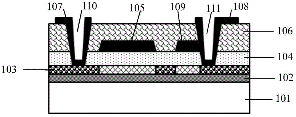
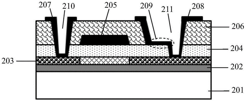
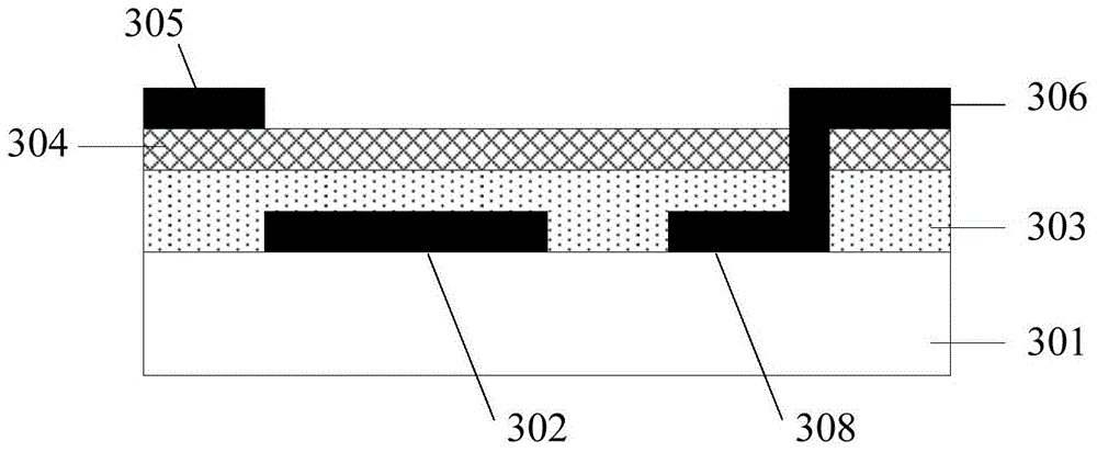
[0058] The thin film transistor (TFT) of the present invention includes: a gate electrode, a source electrode, a drain electrode, an active layer and a gate insulating layer formed on a base substrate, and the gate insulating layer is located between the gate electrode and the active layer Between, the source and the drain are connected to the active layer. In order to reduce the off-state current of the TFT, the TFT further includes an auxiliary gate connected to the drain, and a gate insulating layer is separated between the auxiliary gate and the active layer. That is, an auxiliary TFT connected to the auxiliary gate and drain is formed inside the entire TFT. Due to th...


PUM


Abstract

The invention relates to the technical field of display and discloses a thin film transistor. The thin film transistor comprises a gate, a source, a drain, an active layer and a gate insulation layer which are formed on a substrate, and further comprises an auxiliary gate connected with the drain, wherein the gate insulation layer is arranged between the auxiliary gate and the active layer. The invention further relates to a manufacturing method for the thin film transistor, an array substrate and a display device. The thin film transistor can effectively reduce off-state current.

Description

technical field [0001] The invention relates to the field of display technology, in particular to a thin film transistor and a manufacturing method thereof, an array substrate and a display device. Background technique [0002] Thin-film transistor (TFT) devices used in display panels have a large off-state current due to their own material characteristics. For example, polysilicon is used as the active layer, and there are a large number of defects in the grain boundaries of the polysilicon film, making the grain boundaries It becomes the main "channel" of excessive off-state current, which seriously affects the use effect of TFT. The traditional method for reducing the off-state current is to use the LDD (Lightly Doped Drain) structure, but reducing the off-state current will also result in a lower on-state current, which reduces the off-state current in the case of a large operating voltage. not effectively. Contents of the invention [0003] (1) Technical problems to...

Claims


Application Information

Patent Timeline
IPC IPC(8): H01L29/786H01L21/336H01L29/41H01L21/28
CPCH01L27/1214H01L29/42384H01L29/66484H01L29/78645
Inventor 石磊孙亮许晓伟
Owner BOE TECH GRP CO LTD
Why Eureka
Try Eureka