Photodiode array

A photodiode and array technology, applied in the direction of diodes, circuits, resistors, etc., can solve problems such as voltage drop, achieve the effect of shortening the recovery time and increasing the counting rate

Active Publication Date: 2015-06-24
HAMAMATSU PHOTONICS KK
View PDF6 Cites 12 Cited by
  • Summary
  • Abstract
  • Description
  • Claims
  • Application Information

AI Technical Summary

Problems solved by technology

In the APD pixel where the electron avalanche occurs, the current flows, but a voltage drop occurs in the dropping resistor of several hundred kΩ connected in series to the pixel

Method used


Image

  • Photodiode array
  • Photodiode array
  • Photodiode array

Examples


Embodiment Construction

[0038] Hereinafter, the photodiode array according to the embodiment will be described. In addition, the same symbols are used for the same elements, and overlapping descriptions are omitted.

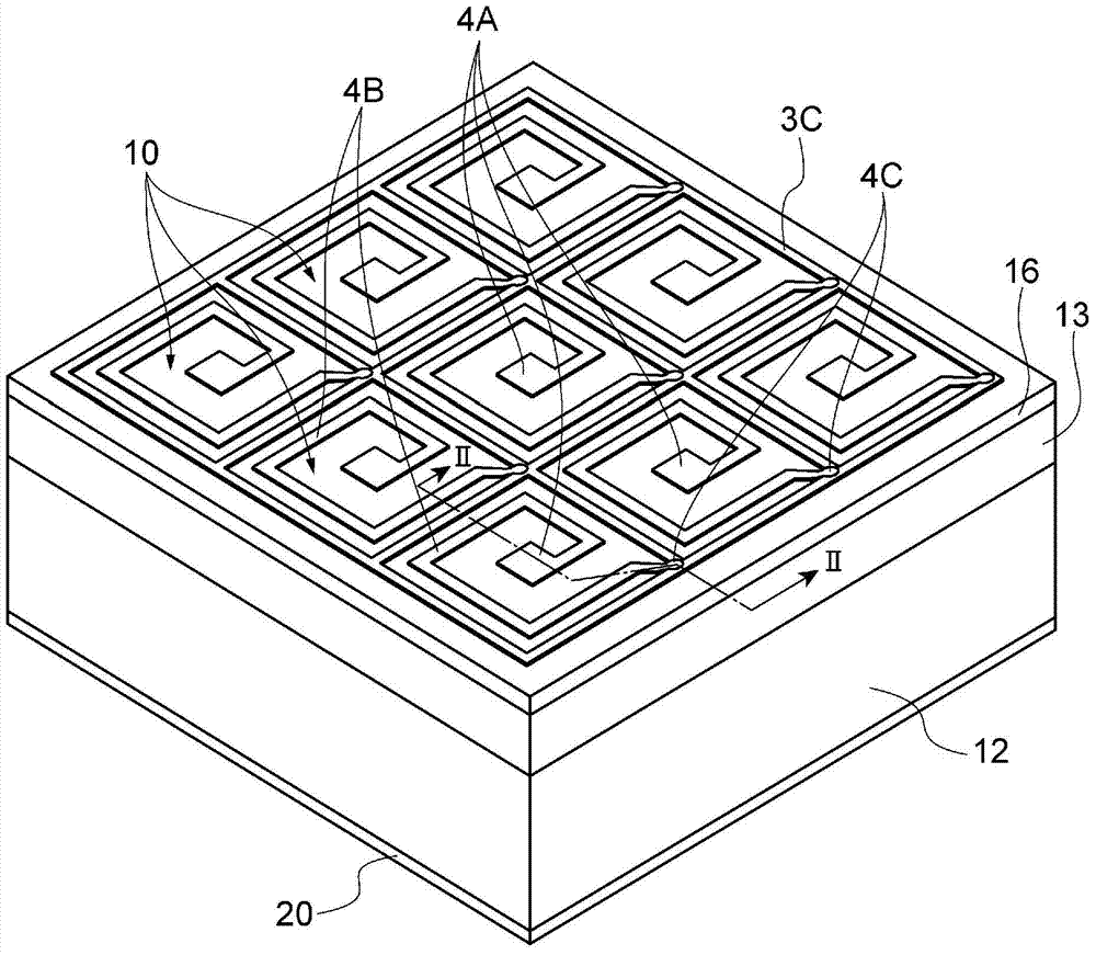
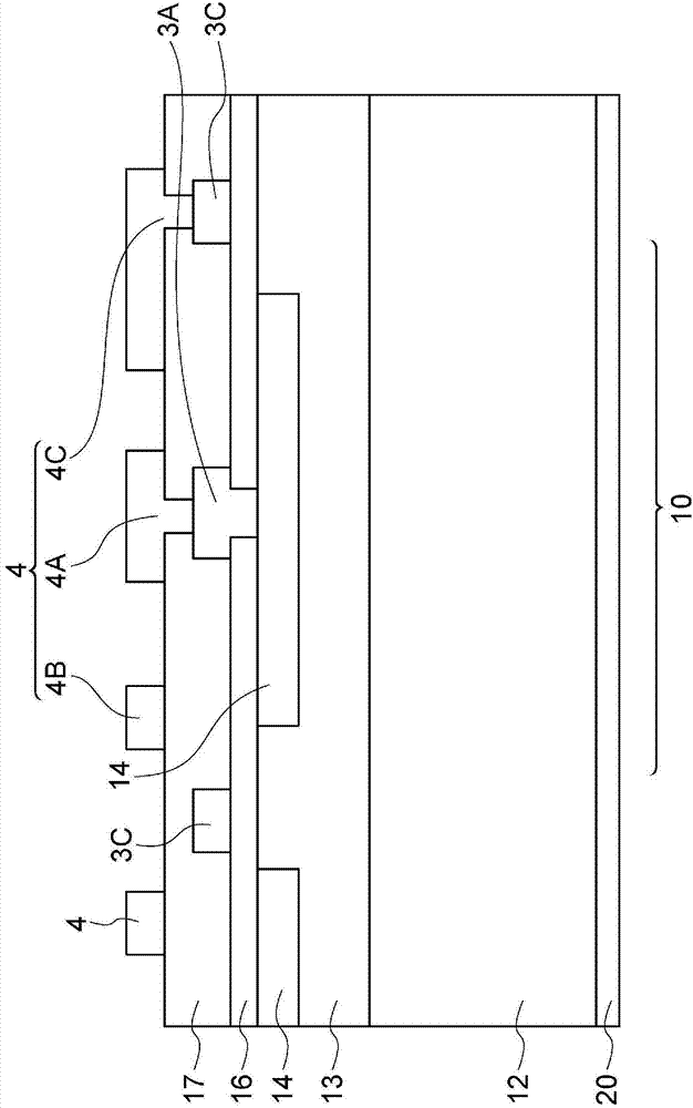
[0039] figure 1 is a perspective view of the photodiode array, figure 2 It is a II-II arrow longitudinal cross-sectional view of a photodiode.

[0040] This photodiode array has a light receiving region on the surface side of a semiconductor substrate made of Si. The light-receiving region includes a plurality of photodetectors (photodetection channels) 10 , and these photodetectors 10 are two-dimensionally arranged in a matrix. In addition, in figure 1 In , the photodetectors 10 are arranged in 9 rows and 9 columns, and these constitute the light-receiving area, but the number of photodetectors 10 can be more or less, and a one-dimensional configuration can also be adopted.

[0041] On the surface of the substrate, a signal readout wiring pattern (upper surface electrode) 3C patt...


PUM


Abstract

A light receiving region includes a plurality of light detecting sections 10. The light detecting sections 10 has a second contact electrode 4A. The second contact electrode 4A is arranged at a position overlapping a first contact electrode 3A, so as to contact the first contact electrode. Further, a resistive layer 4B is continued to the second contact electrode 4A.

Description

technical field [0001] The invention relates to a photodiode array. Background technique [0002] A conventional photodiode array is described in Patent Document 1, for example. In a photodiode array such as SiPM (Silicon Photo Multiplier) or PPD (Pixelated Photon Detector: Pixelated Photon Detector), APDs (Avalanche Photodiodes) are arranged in a matrix, and multiple APDs are connected in parallel and Structure for reading the sum of APD outputs. When the APD is operated in the Geiger mode, weak light (photons) can be detected. That is, when photons are incident on the APD, carriers generated inside the APD are output to the outside through a quenching resistor and a wiring pattern for signal readout. In the pixel of the APD where an electron avalanche occurs, a current flows, but a voltage drop occurs in a dropping resistor of several hundred kΩ connected in series to the pixel. Due to this voltage drop, the voltage applied to the amplification region of the APD is red...

Claims


Application Information

Patent Timeline
Patent Type & Authority Applications(China)
IPC IPC(8): H01L31/107H01L27/146H01L31/00
CPCH01L27/1443H01L27/1446H01L27/14605H01L27/14607H01L27/14609H01L27/14636H01L27/14643H01L28/24H01L31/02027H01L31/022416H01L31/022466H01L31/107
Inventor 山本晃永永野辉昌山村和久里健一土屋龙太郎
Owner HAMAMATSU PHOTONICS KK
Why Eureka
Try Eureka