Supercharge Your Innovation With Domain-Expert AI Agents!

CMOS focal plane readout circuit and signal readout control method

A readout circuit and signal readout technology, applied in the field of CMOS focal plane readout technology, can solve the problems of difficult sampling output of a sampling unit, weak and submerged optical signal output from a pixel, etc., and achieve the effect of extending the dynamic range and improving the sensitivity

Active Publication Date: 2017-10-03
THE 44TH INST OF CHINA ELECTRONICS TECH GROUP CORP
View PDF4 Cites 0 Cited by
  • Summary
  • Abstract
  • Description
  • Claims
  • Application Information

AI Technical Summary

Problems solved by technology

[0003] The problem existing in the prior art is: in the existing focal plane imaging system, multiple pixels in the focal plane array and the sampling unit adopt a one-to-one correspondence connection mode, that is, the output signal of one pixel is processed by one sampling unit; In some occasions, it may appear that the photo-generated signal output by the pixel is relatively weak. At this time, the weak photo-generated signal may be submerged in the noise of the device, making it difficult for the sampling unit to sample and output it.

Method used


Image

  • CMOS focal plane readout circuit and signal readout control method
  • CMOS focal plane readout circuit and signal readout control method
  • CMOS focal plane readout circuit and signal readout control method

Examples


Embodiment Construction

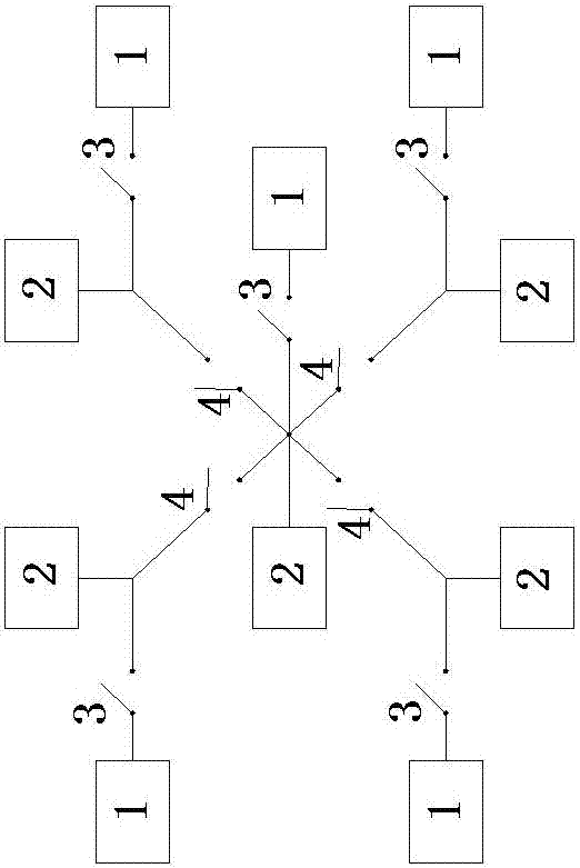
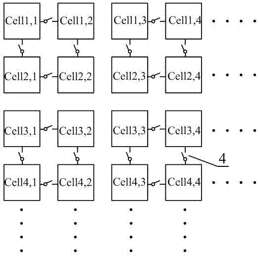
[0016] A CMOS focal plane readout circuit, comprising a two-dimensional focal plane array composed of a plurality of pixels and a CMOS focal plane readout circuit composed of a plurality of sampling units; The input end and the pixel output end are electrically connected through a sampling channel; an input switch is arranged on the sampling channel; the innovation lies in:

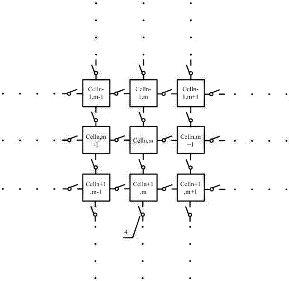
[0017] The position of a certain pixel in the two-dimensional focal plane array is expressed by the label Celln,m, where n represents the number of rows where the pixel is located in the two-dimensional focal plane array, and m represents the pixel in the two-dimensional focal plane array The number of columns in the array; the output end of the pixel marked Celln,m is connected to Celln-1,m, Celln+1,m, Celln,m-1 and Celln,m+ through four connecting wires respectively. The output ends of the four picture elements of 1 are electrically connected; a connection switch is arranged on the connection wire.

[...


PUM


Abstract

A CMOS focal plane readout circuit, the innovation of which is: the position of a certain pixel in the two-dimensional focal plane array is expressed by the mark Celln,m, where n represents the position of the pixel in the two-dimensional focal plane array The number of rows, m represents the column number of the pixel in the two-dimensional focal plane array; then the output terminal of the pixel marked as Celln,m is respectively connected with the cell marked as Celln‑1, m, Celln+1 through four connecting wires ,m, Celln,m‑1 and Celln,m+1 are electrically connected to the output ends of the four picture elements; the connecting wire is provided with a connection switch. The beneficial technical effects of the present invention are: the selective inflow of photo-generated current output by the pixel to the sampling unit can be realized through the switch, the sensitivity of the focal plane imaging system can be improved, and the dynamic range can be expanded.

Description

technical field [0001] The invention relates to a CMOS focal plane readout technology, in particular to a CMOS focal plane readout circuit and a signal readout control method. Background technique [0002] The focal plane imaging system includes a focal plane imaging device (ie, a focal plane array) and a focal plane readout circuit. The basic principle is: the photo-generated current generated by the pixel on the focal plane array is conducted to the sampling unit of the readout circuit through the indium column, and the photo-generated current signal is sampled and integrated by the sampling unit, and then converted into a corresponding voltage signal, and then passed through the sampling unit. The subsequent column-level processing circuit buffers the readout and finally image; common sampling units in the prior art such as capacitive feedback transimpedance amplifier (CTIA) sampling unit, direct injection type (DI) sampling unit, source follower type (SFD) Sampling unit...

Claims


Application Information

Patent Timeline
Patent Type & Authority Patents(China)
IPC IPC(8): H04N5/378H04N5/374
Inventor 李毅强刘昌举吴治军李明祝晓笑
Owner THE 44TH INST OF CHINA ELECTRONICS TECH GROUP CORP
Features
  • R&D
  • Intellectual Property
  • Life Sciences
  • Materials
  • Tech Scout
  • Unparalleled Data Quality
  • Higher Quality Content
  • 60% Fewer Hallucinations
Learn More