
Display panel motherboard and preparation method thereof

A technology for display panels and motherboards, which is used in the identification of devices, instruments, semiconductor devices, etc., can solve problems such as time-consuming and affect the production capacity of the production line, and achieve the effect of improving the production capacity of the production line and optimizing the design space.

Active Publication Date: 2015-07-15
HEFEI BOE OPTOELECTRONIC TECH CO LTD +1
View PDF9 Cites 9 Cited by
  • Summary
  • Abstract
  • Description
  • Claims
  • Application Information

AI Technical Summary

Problems solved by technology

[0004] In order to solve the above problems, the present invention provides a display panel motherboard and a preparation method thereof, which are used to solve the problem in the prior art that it takes a lot of time to mark all the display panels when producing display panels, thereby affecting the production capacity of the production line.

Method used


Image

  • Display panel motherboard and preparation method thereof
  • Display panel motherboard and preparation method thereof
  • Display panel motherboard and preparation method thereof

Examples


Embodiment 1

[0038] The principle of the present invention is to use the positioning mark on the array substrate and the specific number of transition sub-pixels in the non-display area on the side of the display area on the color filter substrate to realize the marking of the display panel.

[0039] When identifying the display panel, the display panel to be identified can be placed under a high-power microscope, and first determined by observing the specific number of transition sub-pixels in the non-display area on the side of the display area on the color filter substrate The process area to which the display panel belongs, and then the specific position of the display panel in the process area is determined by observing the positioning mark on the array substrate, and then the specific position of the display panel in the display panel mother board can be determined.

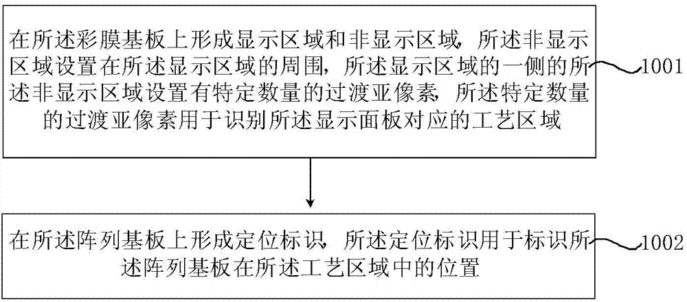
[0040] figure 1 It is a flow chart of a method for manufacturing a display panel motherboard provided by Embodiment 1...

Embodiment 2

[0055] This embodiment provides a motherboard for a display panel, which includes a plurality of process areas, the process areas include a plurality of display panels, and the display panels include a color filter substrate and an array substrate that are oppositely arranged. The color filter substrate includes a display area and a non-display area, the non-display area is arranged around the display area, and the non-display area on one side of the display area is provided with a specific number of transition sub-pixels, so The specific number of transition sub-pixels is used to identify the corresponding process area of ​​the display panel. The array substrate includes a positioning mark, and the positioning mark is used to mark the position of the array substrate in the process area.

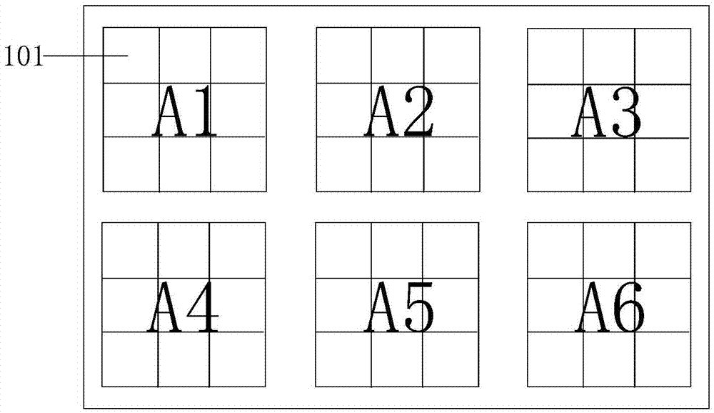
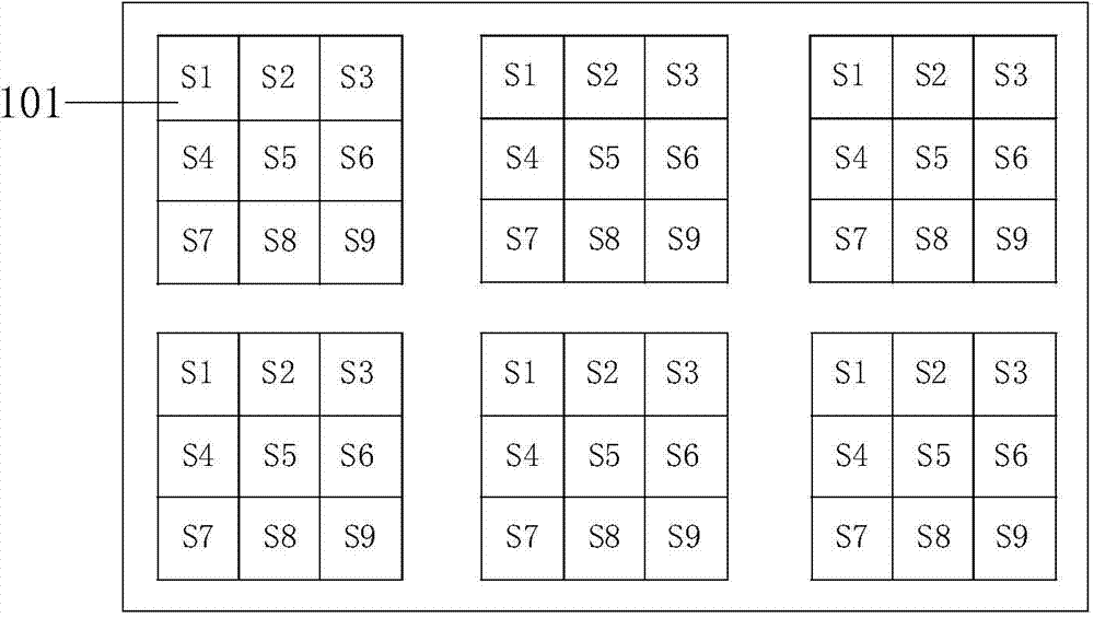
[0056] see figure 2 and image 3 , the display panel includes six process areas 101, namely A1, A2, A3, A4, A5 and A6, and each process area 101 contains nine display panels, namely S1, S...


PUM


Abstract

The invention discloses a display panel motherboard and a preparation method thereof. The display panel motherboard comprises multiple process areas, each process area comprises multiple display panels, and each display panel comprises a color film substrate and an array substrate which are oppositely arranged. According to the technical scheme, the method comprises the steps that the process area to which each display panel belongs is determined through a specified amount of transition subpixels of a non-display area at one side of the display area of the color film substrate, the specific location of a display panel in the process area to which the display panel belongs is judged through a positioning mark on the array substrate, and therefore recognition of the display panels is achieved, the production line capacity is improved, and meanwhile design space of the peripheral zone of a display screen is optimized.

Description

technical field [0001] The invention relates to the field of display technology, in particular to a display panel motherboard and a preparation method thereof. Background technique [0002] Existing display panels are formed by cutting the display panel motherboard, the display panel motherboard is provided with cutting lines, and the cutting lines divide the display panel motherboard into a plurality of display panel units, and the display is completed according to the cutting lines After the panel motherboard is cut, one display panel unit corresponds to one display panel. For the production of large-size display panels, in order to distinguish each display panel, a mark will be set on each display panel unit during the process of making the display panel motherboard. The mark occupies a space of 1cm×10cm, and the display panel motherboard The markings on each display panel unit are different. [0003] For the production of small-sized display panels, hundreds of display...

Claims


Application Information

Patent Timeline
Patent Type & Authority Applications(China)
IPC IPC(8): G09F9/00G02F1/1333G02F1/1335
CPCG02F1/1333G02F1/133514G09F9/00H01L23/544H01L2223/54433H01L2223/54486G02B5/201H01L27/124
Inventor 王辉郭远辉王春陈俊生李小和
Owner HEFEI BOE OPTOELECTRONIC TECH CO LTD
Learn More