Display panel and display device

A display panel and area technology, applied in instruments, nonlinear optics, optics, etc., can solve problems such as low light transmittance, and achieve the effect of large light transmittance area, improved light transmittance, and improved display effect.

Inactive Publication Date: 2015-07-22
SHANGHAI AVIC OPTOELECTRONICS +1
View PDF6 Cites 10 Cited by
  • Summary
  • Abstract
  • Description
  • Claims
  • Application Information

AI Technical Summary

Problems solved by technology

However, the existing self-capacitive touch display devices have low light transmittance

Method used


Image

  • Display panel and display device
  • Display panel and display device
  • Display panel and display device

Examples


Embodiment Construction

[0037] The following will clearly and completely describe the technical solutions in the embodiments of the present invention with reference to the accompanying drawings in the embodiments of the present invention. Obviously, the described embodiments are only some, not all, embodiments of the present invention. Based on the embodiments of the present invention, all other embodiments obtained by persons of ordinary skill in the art without making creative efforts belong to the protection scope of the present invention.

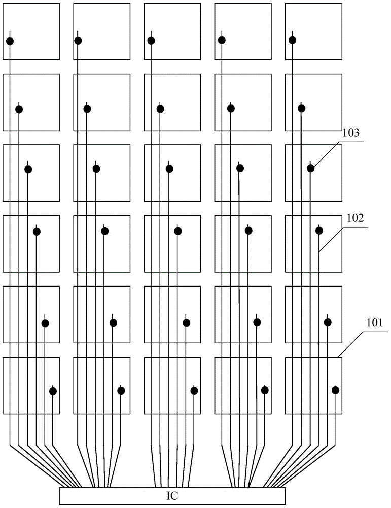
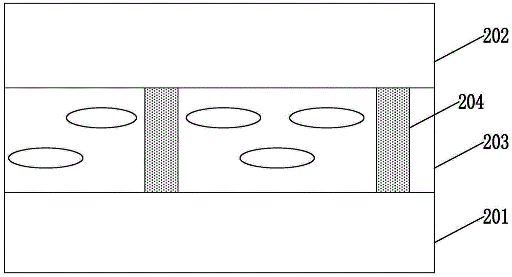
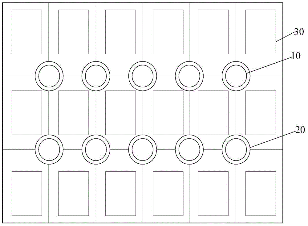
[0038] As mentioned in the background, the existing self-capacitive touch display devices have low light transmittance. The inventors found that the via holes between the lead wires of the touch electrodes and the corresponding touch electrodes affect the light-transmitting area of ​​the array substrate, reducing the light-transmitting area of ​​the array substrate, thereby affecting the light transmittance of the display device, reducing the The display effec...


PUM


Abstract

The invention discloses a display panel and a display device. The display panel comprises a first base board, an array base board, a plurality of touch control electrodes and a plurality of touch control electrode leads, wherein the first base board and the array base board are arranged oppositely, the first base board comprises a plurality of supporting column shielding zones, the array base board comprises a plurality of supporting column containing zones, each supporting column containing zone is located in a projection zone of the corresponding supporting column shielding zone on the array base board, the area of each supporting column shielding zone is larger than the area of the corresponding supporting column containing zone, the touch control electrode leads and the touch control electrodes are arranged on different conducting layers, in addition, each touch control electrode lead is connected with the corresponding touch control electrode through a via hole, and the arrangement zone of each via hole has an overlapping zone with the projection zone of the corresponding column shielding zone on the array base board. Namely, the arrangement zones of the via holes can be partly or fully arranged in the projection zones of the column shielding zones on the array base board, the influence of the arrangement zones of the via holes on the light transmitting area of the array base board is reduced, and the light transmittance of the display device is improved.

Description

technical field [0001] The present invention relates to the technical field of image display, and more specifically, to a display panel and a display device. Background technique [0002] In the initial stage of the development of the touch display, the touch display panel is formed by laminating the touch panel and the display panel to realize the touch display. The touch panel and the display panel need to be prepared separately, the cost is high, the thickness is relatively large, and the production efficiency is low. [0003] With the development of self-capacitive touch display integration technology, the common electrode layer of the array substrate in the display panel can also be used as the touch electrode layer for self-capacitive touch detection, and the touch can be performed in time-sequence through time-sharing driving Control and display control can realize touch and display functions at the same time. In this way, the touch electrodes are directly integrate...

Claims


Application Information

Patent Timeline
Patent Type & Authority Applications(China)
IPC IPC(8): G02F1/1333G02F1/1339G02F1/1343
CPCG02F1/13338G02F1/13394G02F1/134309G02F1/136227
Inventor 金慧俊
Owner SHANGHAI AVIC OPTOELECTRONICS
Why Eureka
Try Eureka