
Crystalline silicon solar cell grid line, electrode and back surface field manufacturing process

A technology for solar cells and crystalline silicon cells, applied in the field of solar power generation, can solve the problems of inability to reach 15 μm, complex manufacturing process, affecting cross-sectional area, etc., and achieve the effects of high photoelectric conversion efficiency, low raw material cost, and large light transmission area.

Inactive Publication Date: 2017-01-25
杨振民 +2
View PDF4 Cites 3 Cited by
  • Summary
  • Abstract
  • Description
  • Claims
  • Application Information

AI Technical Summary

Problems solved by technology

[0005] 1. The production process of silver paste and aluminum paste is complicated, there are many links, and the price is expensive;
[0006] 2. Silver paste and aluminum paste require a large amount of organic chemical materials, which will pollute the environment during production and use;
[0007] 3. The existing production process requires three times of screen printing, two times of oven drying, three times of cooling, and one sintering. The production process is complicated, the production cycle is long, and the cost is increased;
[0008] 4. The polymeric organic solvent in the silver paste and aluminum paste has poor light transmission, and it is difficult to volatilize all through sintering during the sintering process, and there are still some residues, and the resistance value increases, which affects the photoelectric conversion efficiency;
[0009] 5. The width of the existing grid line manufacturing process cannot reach 20 μm, generally 80 μm, which increases the shading area of ​​the battery and affects the conversion efficiency;
[0010] 6. The thickness of the existing grid lines, electrodes, and back electric field can only be 10 μm per screen printing, and cannot reach more than 15 μm, which affects the cross-sectional area

Method used


Image

  • Crystalline silicon solar cell grid line, electrode and back surface field manufacturing process

Examples


Embodiment 1

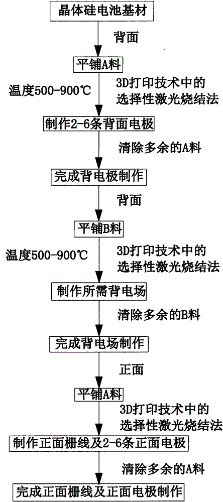
[0031] Embodiment 1: A kind of manufacturing process of crystalline silicon solar cell grid line, electrode, back electric field, it carries out according to following steps:

[0032] Step I: selection of the base material: the present invention selects the crystalline silicon battery that has been processed by processes such as texturing, chemical cleaning, diffusion, etching, dephosphorization, and PECVD as the base material;

[0033] Step II: the production of material A and material B: the present invention uses material A to replace the silver paste in the existing process, and material B to replace the aluminum paste in the existing process. The material A has a high expansion coefficient, low melting point, transparent Glass-ceramic powder with good light properties and silver powder are mixed in a certain proportion. The ratio of silver powder to glass-ceramic powder is 9:1. Material B is made of glass-ceramic powder and aluminum powder in a certain proportion. Aluminum...

Embodiment 2

[0038] Embodiment 2: A kind of manufacturing process of crystalline silicon solar cell grid line, electrode, back electric field, it is carried out according to following steps:

[0039] Step I: selection of the base material: the present invention selects the crystalline silicon battery that has been processed by processes such as texturing, chemical cleaning, diffusion, etching, dephosphorization, and PECVD as the base material;

[0040] Step II: the production of material A and material B: the present invention uses material A to replace the silver paste in the existing process, and material B to replace the aluminum paste in the existing process. The material A has a high expansion coefficient, low melting point, transparent Glass-ceramic powder with good light properties and silver powder are mixed in a certain proportion. The ratio of silver powder to glass-ceramic powder is 18:1. Material B is made of glass-ceramic powder and aluminum powder in a certain proportion. The...

Embodiment 3

[0045]Embodiment 3: a kind of manufacturing process of crystalline silicon solar cell grid line, electrode, back electric field, it is carried out according to following steps:

[0046] Step I: selection of the base material: the present invention selects the crystalline silicon battery that has been processed by processes such as texturing, chemical cleaning, diffusion, etching, dephosphorization, and PECVD as the base material;

[0047] Step II: the production of material A and material B: the present invention uses material A to replace the silver paste in the existing process, and material B to replace the aluminum paste in the existing process. The material A has a high expansion coefficient, low melting point, transparent Glass-ceramic powder with good light properties and silver powder are mixed in a certain proportion. The ratio of silver powder to glass-ceramic powder is 14:1. Material B is made of glass-ceramic powder and aluminum powder in a certain proportion. The ...


PUM

PropertyMeasurementUnit
widthaaaaaaaaaa
particle diameteraaaaaaaaaa

Abstract

The invention discloses a crystalline silicon solar cell grid line, electrode and back surface field manufacturing process. A crystalline silicon cell subjected to processes of texturizing, chemical cleaning, diffusing, etching, dephosphorizing, PECVD (plasma enhanced chemical vapor deposition) and the like serves as a base material; silver paste in the prior art is replaced with a material A, and aluminum paste in the prior art is replaced with a material B; a selective laser sintering method in the 3D printing technology is adopted for crystalline silicon solar cell grid line, electrode and back surface field manufacture. The manufacturing process has advantages that manufactured solar cells are large in light transmittance area, low in resistance, high in conductivity and high in photoelectric conversion efficiency; discharging of chemical substances in a manufacturing process is avoided, so that environment friendliness is realized; by adoption of glass ceramic powder which is a lead-free material, environment pollution is avoided; technical simplicity, easiness in operation and high production efficiency are realized; raw materials are low in cost.

Description

technical field [0001] The invention relates to a manufacturing process of grid lines, electrodes and back electric fields of crystalline silicon solar cells, belonging to the field of solar power generation. Background technique [0002] After decades of development, the crystalline silicon solar power generation industry has become a systematic project, and a complete production system has also been built. For example, the silicon wafer determines the initial photoelectric conversion efficiency, and the fabrication of grid lines, electrodes, and back electric field is the key factor for the electrical energy export efficiency. [0003] At present, the grid lines, electrodes, and back electric field manufacturing process of mainstream solar cells are mainly to print the grid lines and electrodes on the front of the battery with silver paste by silk screen printing, then dry and cool in a drying oven, and then print electrodes on the back, and dry them in a drying oven. Aft...

Claims


Application Information

Patent Timeline
Patent Type & Authority Applications(China)
IPC IPC(8): H01L31/0224H01L31/18
CPCH01L31/022425H01L31/18Y02E10/50Y02P70/50
Inventor 杨振民杨嘉兴白庆辉
Owner 杨振民
Learn More