

Thin film transistor array substrate, and manufacturing method and liquid crystal display apparatus thereof,
A thin film transistor and array substrate technology, applied in the field of liquid crystal display, can solve the problems of harsh process conditions, low yield, low transmittance and aperture ratio of new materials and new technologies, and achieves increased transmittance and good connection performance. , the effect of reducing the drain pattern
- Summary
- Abstract
- Description
- Claims
- Application Information
AI Technical Summary
Problems solved by technology
Method used
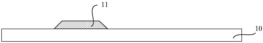
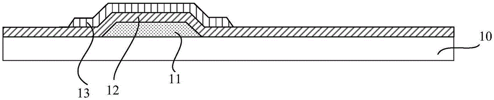
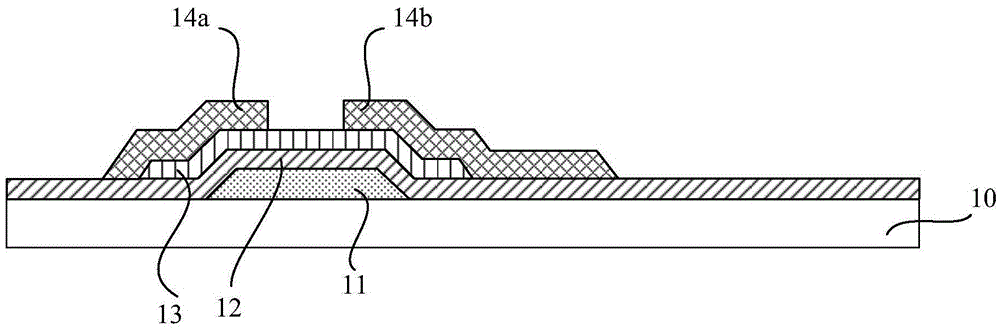
Image

Examples
Embodiment Construction
[0044] The present invention is described below based on examples, but the present invention is not limited to these examples. In the following detailed description of the invention, some specific details are set forth in detail. The present invention can be fully understood by those skilled in the art without the description of these detailed parts. In order not to obscure the essence of the present invention, well-known methods, procedures, procedures, components and circuits have not been described in detail.
[0045] Additionally, those of ordinary skill in the art will appreciate that the drawings provided herein are for illustrative purposes and are not necessarily drawn to scale.
[0046] Unless the context clearly requires, throughout the specification and claims, "comprises", "comprises" and similar words should be interpreted in an inclusive sense rather than an exclusive or exhaustive meaning; that is, "including but not limited to" meaning.
[0047] In the descr...
PUM
 Abstract
Description
Claims
Application Information