Light emitting device with beveled reflector and manufacturing method of the same

a technology of light emitting devices and reflectors, which is applied in the direction of semiconductor devices, basic electric elements, electrical appliances, etc., can solve the problems of poor heat dissipation, poor spatial color uniformity, and complicating the design of secondary optical lenses, so as to improve the efficiency of light extraction and improve the spatial color uniformity , the effect of reducing the irradiation area

Active Publication Date: 2017-04-06
MAVEN OPTRONICS CO LTD
View PDF3 Cites 24 Cited by
  • Summary
  • Abstract
  • Description
  • Claims
  • Application Information

AI Technical Summary

Benefits of technology

[0010]One object of some embodiments of the present disclosure is to provide a light emitting device and a manufacturing method thereof, to achieve better light extraction efficiency, improved spatial

Problems solved by technology

However, there are intrinsic limitations in PLCC-type LEDs, including: 1) Poor spatial color uniformity, due to large variations of the lengths along various optical paths of different light emitting angles, which will result in a projected yellow ring or a blue ring; 2) The light emitting surface area of a PLCC-type phosphor-converted light emitting device is significantly larger than that of a LED semiconductor die that is bonded inside the package.
A larger light emitting surface area will result in larger etendue of the LED as a light source and complicates the design of a secondary optical lens accordingly; and 3) PLCC-type LED package has poor heat dissipation due to relatively higher thermal resistance between the LED semiconductor die and a lead frame.
However, some of the good optical properties commonly found in conventional PLCC-type LED packages are lost for CSP-type LEDs due to continuous shrinkage of the package size.
For example, for those CSP-type LEDs, four edge surfaces of a photoluminescent str

Method used


Image

  • Light emitting device with beveled reflector and manufacturing method of the same
  • Light emitting device with beveled reflector and manufacturing method of the same
  • Light emitting device with beveled reflector and manufacturing method of the same

Examples


Embodiment Construction

Definitions

[0038]The following definitions apply to some of the technical aspects described with respect to some embodiments of the invention. These definitions may likewise be expanded upon herein.

[0039]As used herein, the singular terms “a,”“an,” and “the” include plural referents unless the context clearly dictates otherwise. Thus, for example, reference to a layer can include multiple layers unless the context clearly dictates otherwise.

[0040]As used herein, the term “set” refers to a collection of one or more components. Thus, for example, a set of layers can include a single layer or multiple layers. Components of a set also can be referred to as members of the set. Components of a set can be the same or different. In some instances, components of a set can share one or more common characteristics.

[0041]As used herein, the term “adjacent” refers to being near or adjoining. Adjacent components can be spaced apart from one another or can be in actual or direct contact with one a...


PUM


Abstract

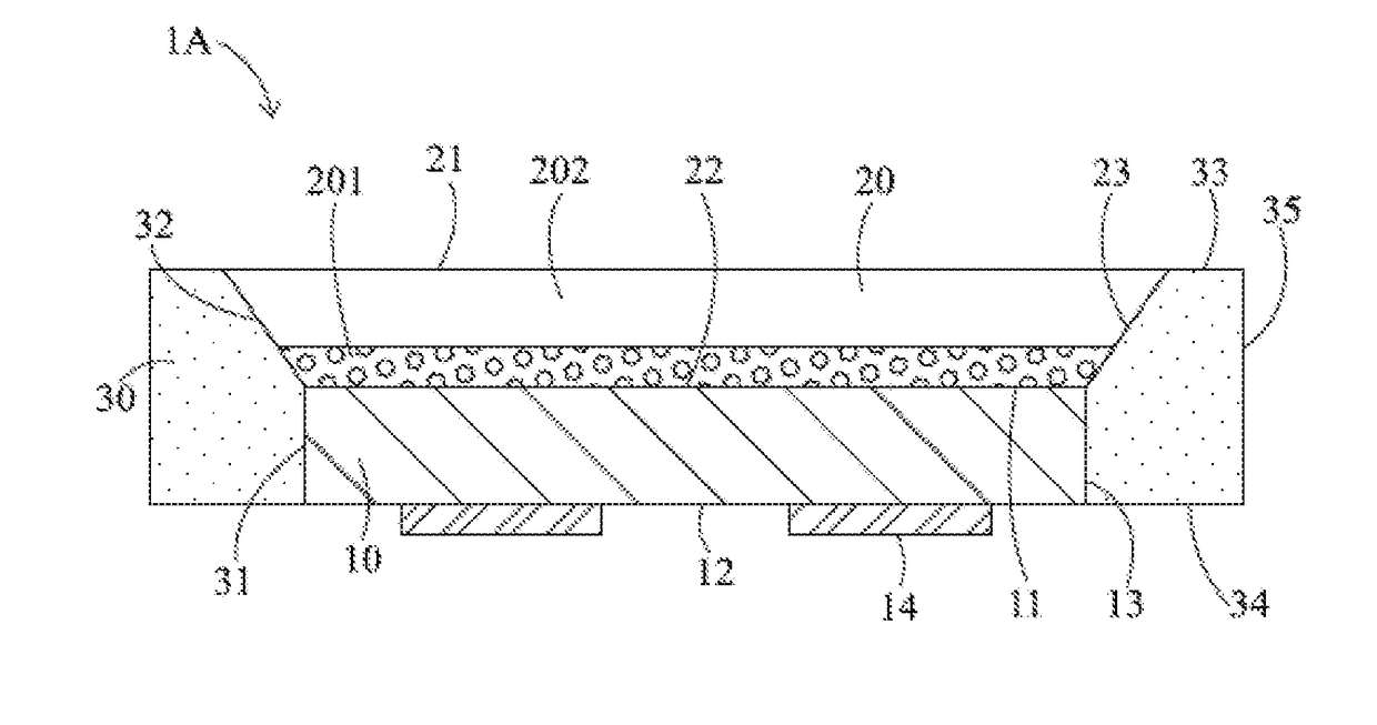
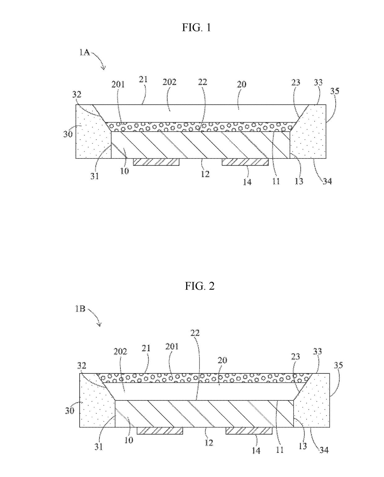
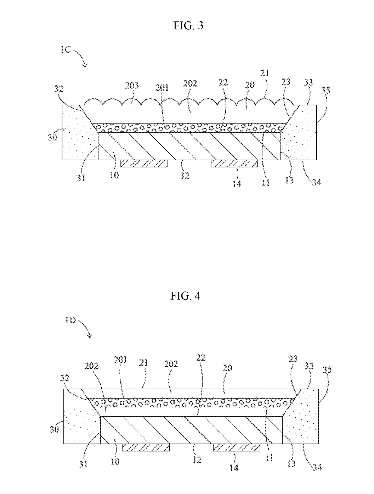
A light emitting device, including an LED semiconductor die, a photoluminescent structure and a reflector, is disclosed. The photoluminescent structure with a beveled edge surface is disposed on top of the LED semiconductor die, wherein a lower surface of the photoluminescent structure adheres to an upper surface of the LED semiconductor die. A reflective resin material is disposed surrounding edge surfaces of the LED semiconductor die and the photoluminescent structure forming a beveled reflector. A method to manufacture the above light emitting device is also disclosed. Advantages of this light emitting device with beveled reflector include increasing the light extraction efficiency, making the viewing angle tunable, improving spatial color uniformity and reducing the light source etendue realized in a compact form-factor size.

Description

CROSS-REFERENCES TO RELATED APPLICATIONS[0001]This application claims the benefit of and priority to Taiwan Patent Application No. 104132711 filed on Oct. 5, 2015, and Chinese Patent Application No. 201610033451.4 filed on Jan. 19, 2016, which also claims priority to the Taiwan Patent Application, the disclosures of which are incorporated herein by reference in their entirety.BACKGROUND[0002]Technical Field[0003]The present disclosure relates to a light emitting device and the manufacturing method thereof, in particular to a chip-scale packaging light emitting device including a light emitting diode (LED) semiconductor die which generates electromagnetic radiation while it is in operation.[0004]Description of the Related Art[0005]In the past decades, LEDs are widely used in applications including signal lamps, backlight units, general lightings, mobile components, automotive lightings and so forth. Generally an LED semiconductor die is disposed within a package structure, and / or cov...

Claims


Application Information

Patent Timeline
IPC IPC(8): H01L33/50H01L33/60
CPCH01L33/507H01L2933/0058H01L2933/0041H01L33/60H01L33/46H01L33/486H01L33/505H01L33/58H01L2933/0033H01L33/56
Inventor CHEN, CHIEHWANG, TSUNG-HSI
Owner MAVEN OPTRONICS CO LTD
Why Eureka
Try Eureka