
Display panel and manufacturing method thereof

A technology for display panels and substrates, which is used in the manufacture of semiconductor/solid-state devices, electrical components, and electrical solid-state devices, etc., and can solve the problems of less light-transmitting area and low transparency of the panel.

Inactive Publication Date: 2020-06-12
SHENZHEN CHINA STAR OPTOELECTRONICS SEMICON DISPLAY TECH CO LTD
View PDF4 Cites 4 Cited by
  • Summary
  • Abstract
  • Description
  • Claims
  • Application Information

AI Technical Summary

Problems solved by technology

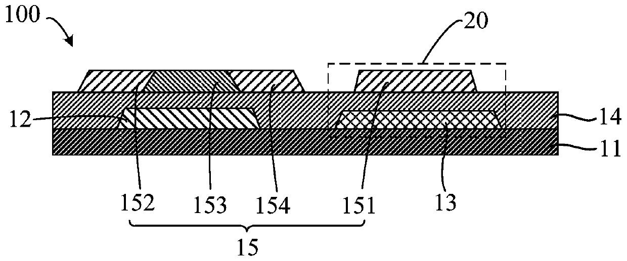
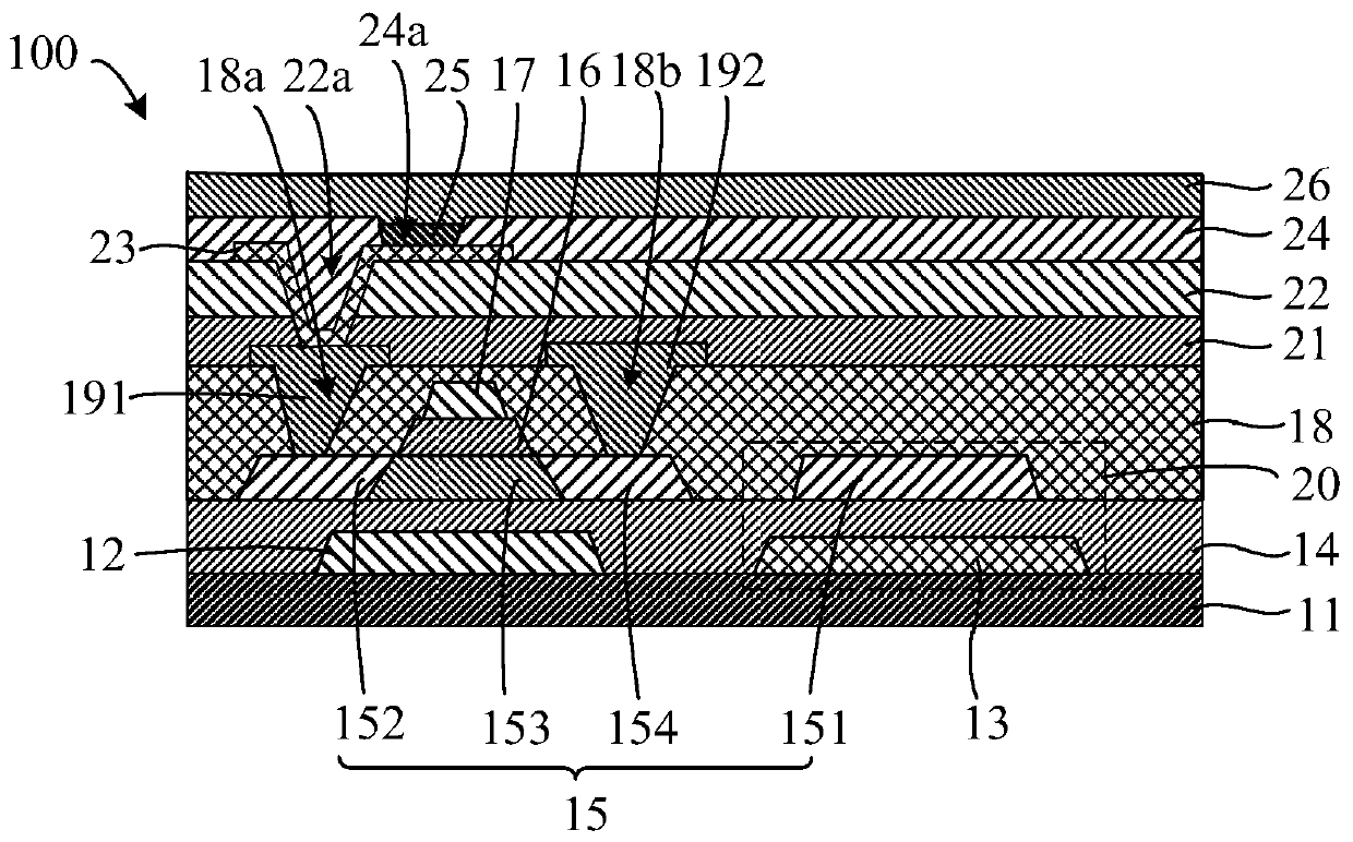
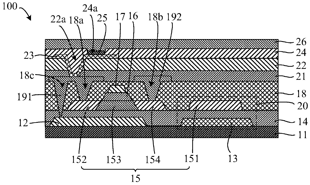
[0003] Embodiments of the present application provide a display panel and a manufacturing method thereof to solve the technical problem that the display panel has less light-transmitting areas and low transparency

Method used


Image

  • Display panel and manufacturing method thereof
  • Display panel and manufacturing method thereof
  • Display panel and manufacturing method thereof

Examples


Embodiment Construction

[0032] The following will clearly and completely describe the technical solutions in the embodiments of the application with reference to the drawings in the embodiments of the application. Apparently, the described embodiments are only some of the embodiments of the application, not all of them. Based on the embodiments in this application, all other embodiments obtained by those skilled in the art without making creative efforts belong to the scope of protection of this application.

[0033] In the description of the present application, it should be understood that the orientation or positional relationship indicated by the terms "thickness", "upper", "lower", "vertical", "one side" etc. is based on the orientation or position shown in the drawings The relationship is only for the convenience of describing the present application and simplifying the description, but does not indicate or imply that the referred device or element must have a specific orientation, be constructe...


PUM

PropertyMeasurementUnit
Thicknessaaaaaaaaaa
Thicknessaaaaaaaaaa

Abstract

The invention discloses a display panel and a manufacturing method thereof. The display panel comprises a substrate; a shading metal block and a transparent conductive block arranged on the substrate;a buffer layer arranged on the substrate, the shading metal block and the transparent conductive block; an active layer pattern arranged on the buffer layer, wherein the active layer pattern comprises a first conductive block, the first conductive block and the transparent conductive block are oppositely arranged, the first conductive block is formed by conducting a semiconductor material, and the transparent conductive block and the first conductive block form two poles of a capacitor. According to the scheme, the light-transmitting area of the display panel can be effectively increased, andthe transparency of the display panel is improved.

Description

technical field [0001] The present application relates to the field of display technology, in particular to a display panel and a manufacturing method thereof. Background technique [0002] The transmittance of the display panel plays an extremely important role in its overall display performance. The higher the transmittance, the higher the display brightness and the better the transparency of the display panel. The structure of the display panel usually includes a thin film transistor (Thin Film Transistor, TFT) and a capacitor. In the prior art, a metal layer and an ion-doped semiconductor layer are usually used to form the two poles of the capacitor, but since the metal layer is opaque, it reduces The light-transmitting area of ​​the display panel is restricted, so that the transparency of the display panel is not high. Contents of the invention [0003] Embodiments of the present application provide a display panel and a manufacturing method thereof, so as to solve t...

Claims


Application Information

Patent Timeline
IPC IPC(8): H01L27/12H01L21/77H01L27/32
CPCH01L27/1255H01L27/1259H10K59/1315H10K59/8792H10K59/126H10K59/1213H01L29/78633H10K50/865H10K71/00H10K2102/102H10K2102/103
Inventor 周星宇
Owner SHENZHEN CHINA STAR OPTOELECTRONICS SEMICON DISPLAY TECH CO LTD
Learn More