Optical device and manufacturing method therefor

A processing method and technology for optical devices, which are applied in the fields of semiconductor devices, semiconductor/solid-state device manufacturing, electrical components, etc., can solve the problems of reduced brightness and reduced light export efficiency, and achieve the effect of improving export efficiency.

Inactive Publication Date: 2015-07-29
DISCO CORP
View PDF11 Cites 7 Cited by
  • Summary
  • Abstract
  • Description
  • Claims
  • Application Information

AI Technical Summary

Problems solved by technology

As a result, there is a problem that the light extraction efficiency in the optical device is lowered, resulting in a lowered luminance.

Method used


Image

  • Optical device and manufacturing method therefor
  • Optical device and manufacturing method therefor
  • Optical device and manufacturing method therefor

Examples


Embodiment Construction

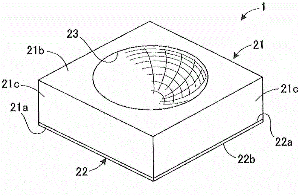
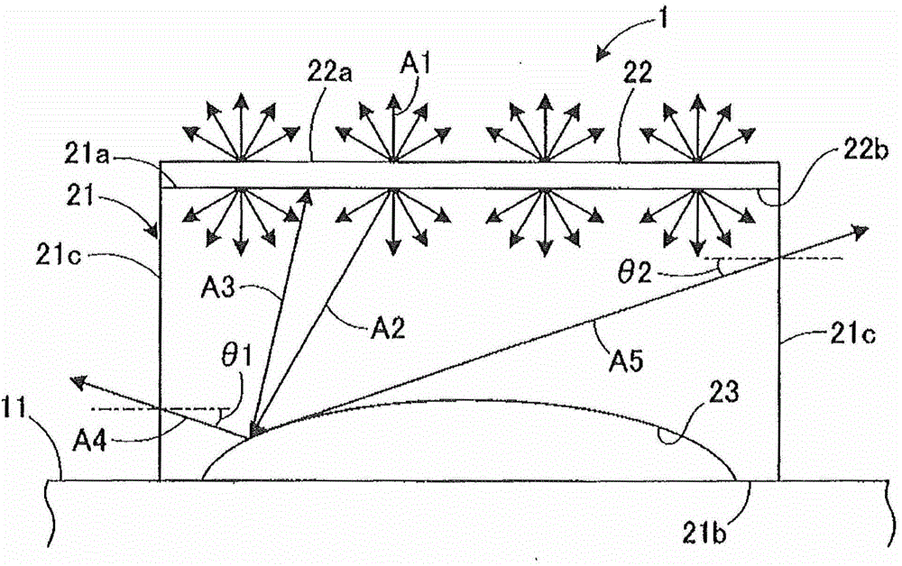
[0031] The optical device and its processing method will be described with reference to the drawings. First, refer to figure 1 and figure 2 , Describe the optical device. figure 1 It is a perspective view showing an example of the optical device from the back side. figure 2 It is a cross-sectional view for explaining the light emission state of the optical device.

[0032] Such as figure 1 and figure 2 As shown, the optical device 1 is wire-bonded or flip-chip packaged on the base 11 (in figure 1 Not shown in the middle). The optical device 1 is configured to include a substrate 21 and a light-emitting layer 22 formed on the front surface 21 a of the substrate 21. The substrate 21 is used as a substrate for crystal growth, from a sapphire substrate (Al 2 O 3 Substrate), gallium nitride substrate (GaN substrate), silicon carbide substrate (SiC substrate), gallium oxide substrate (Ga 2 O 3 Substrate) to select. The substrate 21 is preferably transparent.

[0033] The light-emitt...


PUM


Abstract

An optical device including a substrate and a light emitting layer formed on the front surface of the substrate. The back surface of the substrate is formed with a concave portion like a crater. The concave portion is formed by applying a laser beam having an absorption wavelength to an optical device wafer. In the optical device, light emitted from the light emitting layer strikes the inner surface of the concave portion and is next irregularly reflected from the inner surface of the concave portion.

Description

Technical field [0001] The present invention relates to an optical device having a light-emitting layer formed on the front surface of a substrate and a processing method of the optical device. Background technique [0002] In the manufacturing process of optical devices such as laser diodes (LD) and light emitting diodes (LED), a light-emitting layer (epitaxial layer) is laminated by, for example, epitaxial growth on the upper surface of a crystal growth substrate made of sapphire or SiC (silicon carbide). Thus, an optical device wafer for forming a plurality of optical devices is manufactured. Optical devices such as LD and LED are formed on the front surface of the optical device wafer in each area divided by a plurality of planned division lines configured in a grid shape, and the optical device wafer is divided into a single piece by dividing the optical device wafer along the planned division lines. In this way, one optical device is manufactured. [0003] Conventionally, a...

Claims


Application Information

Patent Timeline
Patent Type & Authority Applications(China)
IPC IPC(8): H01L33/22H01L33/00
CPCH01L33/24H01L33/005H01L33/0095H01L33/20H01L21/76H01L21/78
Inventor 桐原直俊相川力伊藤优作荒川太郎杨子君
Owner DISCO CORP
Why Eureka
Try Eureka