Thin-film solar cell and p-type semiconductor and preparation method of p-shaped semiconductor

A solar cell and semiconductor technology, applied in semiconductor devices, circuits, photovoltaic power generation, etc., can solve the problems of increasing the additional absorption of incident light, large light-induced attenuation, etc., to achieve increased fill factor, short-circuit current and open-circuit voltage, battery The effect of improving conversion efficiency

Inactive Publication Date: 2013-04-10
FENGFAN
View PDF9 Cites 3 Cited by
  • Summary
  • Abstract
  • Description
  • Claims
  • Application Information

AI Technical Summary

Problems solved by technology

The first approach often leads to greater light-induced attenuation, while the second approach increases the additional absorption of incident light in the window layer

Method used


Image

  • Thin-film solar cell and p-type semiconductor and preparation method of p-shaped semiconductor
  • Thin-film solar cell and p-type semiconductor and preparation method of p-shaped semiconductor
  • Thin-film solar cell and p-type semiconductor and preparation method of p-shaped semiconductor

Examples


Embodiment Construction

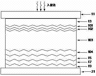
[0033] Such as figure 1 The single-junction amorphous silicon a-Si:H thin-film solar cell shown has the front transparent insulating substrate 11 as the light incident side, and from the light incident side, the front electrodes are laminated in sequence: transparent conductive film 13, p+ layer Amorphous silicon carbide a-SiC:H film 101, p-layer amorphous silicon carbide a-SiC:H film 102, i-layer amorphous silicon a-Si:H intrinsic absorption layer 103, n-layer amorphous silicon a- Si:H thin film 104 , first back electrode layer 15 , second back electrode layer 17 , filling material layer 19 and back transparent insulating plate 21 .

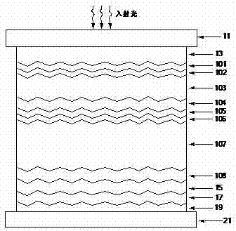
[0034] Such as figure 2 The shown double-junction amorphous silicon a-Si:H / a-Si:H thin-film solar cell uses the front transparent insulating substrate 11 as the light-incident side, and starts from the light-incident side to stack the front electrodes sequentially: transparent Conductive film 13, first junction p+ layer amorphous silicon car...


PUM


Abstract

The invention discloses a thin-film solar cell and a p-type semiconductor and a preparation method of the p-shaped semiconductor. The thin-film solar cell is in a single-junction or a double-junction or a multi-junction structure having more than three junctions. The thin-film solar cell is formed by the p-shaped semiconductor which comprises a p<+> layer semiconductor thin film and a p<-> layer semiconductor thin film. As for a amorphous silicon cell, both the p+layer semiconductor thin film and the p<-> semiconductor thin film are amorphous silicon carbide a-Si C:H thin films. As for a microcrystalline silicon cell, both the p<+> layer semiconductor thin film and the p-layer semiconductor thin film are microcrystalline silicon mu-Si:H thin films. The p-shaped semiconductor not only enables more useful light to enter into an i-layer, the intrinsic absorption layer through the p-shaped semiconductor, but also is capable of contacting perfectly with a front electrode or a front junction cell so as to improve the export efficiency of an electron hole to the maximum extent. By improving from two aspects of the utilization efficiency of the solar spectrum and the carrier collection efficiency, the energy conversion efficiency of the photovoltaic cell prepared by the p-shaped semiconductor can be improved.

Description

technical field [0001] The invention relates to a thin-film solar cell, a p-type semiconductor made thereof and a preparation method of the p-type semiconductor. Background technique [0002] Thin-film solar cells represent the development trend of photovoltaic power generation technology due to their low energy consumption, low cost, large area integration and high conversion efficiency. Silicon-based thin-film solar cells currently occupy the largest market share of thin-film photovoltaic cells, and are generally prepared by PECVD (plasma-enhanced chemical vapor deposition) equipment using source gases containing silane. Single-junction silicon-based thin-film cells usually show a p-i-n structure, boron-doped silicon film (p layer) as the window region, undoped intrinsic silicon film (i layer) as the light absorption region, phosphorus-doped silicon film (n layer) ) is used to form a built-in electric field, and a transparent conductive oxide film is used as the front ele...

Claims


Application Information

Patent Timeline
Patent Type & Authority Applications(China)
IPC IPC(8): H01L31/0352H01L31/0376H01L31/075H01L31/076H01L31/20
CPCY02E10/548Y02P70/50
Inventor 高平奇孔英王宽冒黄艳红云骁健
Owner FENGFAN
Why Eureka
Try Eureka