Laminated organic thin-film solar cell and preparation method thereof

A technology of solar cells and organic thin films, applied in circuits, photovoltaic power generation, electrical components, etc., can solve problems such as limiting the energy conversion efficiency of tandem cells

Inactive Publication Date: 2011-06-08
UNIV OF ELECTRONICS SCI & TECH OF CHINA
View PDF6 Cites 46 Cited by
  • Summary
  • Abstract
  • Description
  • Claims
  • Application Information

AI Technical Summary

Problems solved by technology

Therefore, the relatively small current of the front cell limits the current of the whole tandem org

Method used


Image

  • Laminated organic thin-film solar cell and preparation method thereof
  • Laminated organic thin-film solar cell and preparation method thereof
  • Laminated organic thin-film solar cell and preparation method thereof

Examples


Embodiment 1

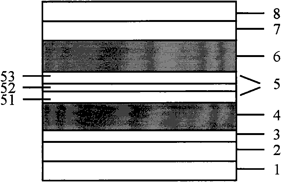
[0052] Such as figure 2 As shown, the connection layer in the device structure includes an anti-reflection film and a hole transport layer, and the material of the anti-reflection film is TiO 2 , the hole transport layer material is MoO 3 , the transparent anode material is ITO, and the anode buffer layer material is MoO 3 , the organic photoelectric conversion layer 1 is SubPc / C 60 Heterojunction, organic photoelectric conversion layer 2 is SubNc / C 60 Heterojunction, the cathode buffer layer material is Bphen.

[0053] Glass substrate / ITO / MoO 3 (5nm) / SubPc(16nm) / C 60 (30nm) / TiO 2 (5nm) / MoO 3 (5nm) / SubNc(10nm) / C60 (30nm) / Bphen(3nm) / Ag(100nm)

[0054] The preparation method is as follows:

[0055] ①Use ethanol solution, acetone solution and deionized water to ultrasonically clean the transparent conductive substrate ITO glass, and dry it with dry nitrogen after cleaning. Wherein the ITO film on the glass substrate is used as the cathode layer of the device, the squar...

Embodiment 2

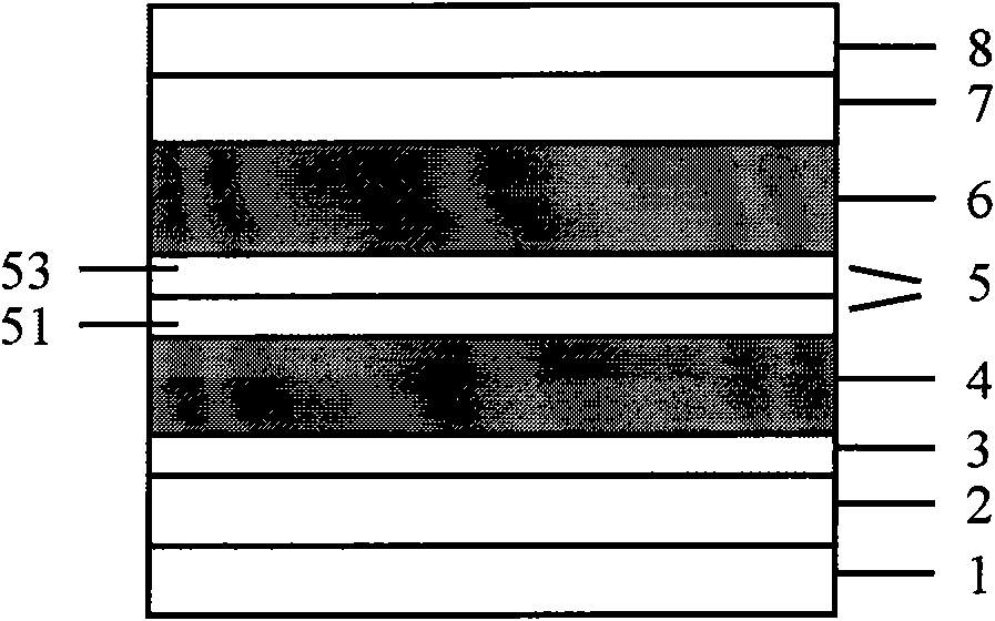
[0070] Such as Image 6 As shown, the connection layer in the device structure includes an anti-reflection film, a thin metal layer and a hole transport layer, and the material of the anti-reflection film is TiO 2 , the thin metal layer is Ag, and the hole transport layer material is MoO 3 , the transparent anode material is ITO, and the anode buffer layer material is MoO 3 , the organic photoelectric conversion layer 1 is SubPc / C 60 Heterojunction, organic photoelectric conversion layer 2 is SubNc / C 60 Heterojunction, cathode buffer layer material is Bphen

[0071] Glass substrate / ITO / MoO 3 (5nm) / SubPc(16nm) / C 60 (30nm) / TiO 2 (5nm) / Ag(0.2nm) / MoO 3 (5nm) / SubNc(10nm) / C 60 (30nm) / Bphen(3nm) / Ag(100nm)

[0072] The preparation method is as follows:

[0073] ①Use ethanol solution, acetone solution and deionized water to ultrasonically clean the transparent conductive substrate ITO glass, and dry it with dry nitrogen after cleaning. Wherein the ITO film on the glass subst...

Embodiment 3

[0079] Such as figure 2 As shown, the connection layer in the device structure includes an anti-reflection film and a hole transport layer, and the material of the anti-reflection film is TiO 2 , the hole transport layer material is MoO 3 , the transparent anode material is ITO, and the anode buffer layer material is MoO 3 , the organic photoelectric conversion layer 1 is a P3HT:PCBM bulk heterojunction, the organic photoelectric conversion layer 2 is a PSBTBT:PCBM bulk heterojunction, and the material of the cathode buffer layer is Bphen

[0080] Glass substrate / ITO / MoO 3 (5nm) / P3HT:PCBM(150nm) / TiO 2 (10nm) / MoO 3 (5nm) / PSBTBT:PCBM(120nm) / Bphen(3nm) / Ag(100nm)

[0081] The preparation method is as follows:

[0082] ①Use ethanol solution, acetone solution and deionized water to ultrasonically clean the transparent conductive substrate ITO glass, and dry it with dry nitrogen after cleaning. Wherein the ITO film on the glass substrate is used as the cathode layer of the de...


PUM

PropertyMeasurementUnit
Thicknessaaaaaaaaaa
Thicknessaaaaaaaaaa
Wavelengthaaaaaaaaaa

Abstract

The invention discloses a laminated organic thin-film solar cell comprising a substrate, a transparent anode layer, an anode buffering layer, an organic photoelectric conversion layer 1, a connecting layer, an organic photoelectric conversion layer 2, a cathode buffering layer and a cathode layer, wherein the connecting layer can be formed by the following two methods: (1) an enhancement reflection film and a hole transporting layer are combined into the connecting layer; and (2) an enhancement reflection film, a metal thin layer and a hole transporting layer are combined into the connecting layer. The enhancement reflection film can improve the reflectivity of the connecting layer according to the specified range of wavelength. Simultaneously, the enhancement reflection film has better electronic transmission performance, guarantees electrons and holes to be effectively compounded on the connecting layer. The laminated organic thin-film solar cell prepared by the method is characterized by high energy conversion efficiency and good stability.

Description

technical field [0001] The invention relates to the technical field of organic photoelectric devices in electronic components, in particular to a stacked organic thin film solar cell and a preparation method thereof. Background technique [0002] In the 21st century, with the rapid development of modern industry, human beings are facing the dual pressure of energy reduction and environmental pollution. In 1954, Bell Laboratories reported a solar cell with a photoelectric conversion efficiency of 6%, marking the beginning of practical solar energy research and creating the first case of photoelectric conversion. At present, the energy conversion efficiency of inorganic solar cells has reached more than 40.7%. Although inorganic solar cells have been commercialized for a long time, their processing technology is complicated, the material requirements are harsh, and the cost is too high. At the same time, the conversion efficiency of its mature technology has basically reache...

Claims


Application Information

Patent Timeline
IPC IPC(8): H01L51/42H01L51/44H01L51/46H01L51/48
CPCY02E10/549Y02E10/50
Inventor 于军胜臧月王娜娜黄江蒋亚东
Owner UNIV OF ELECTRONICS SCI & TECH OF CHINA
Why Eureka
Try Eureka