Method for fine-hair maring using monocrystalline silicon slice

A monocrystalline silicon wafer and texturing technology, which is applied in the fields of final product manufacturing, sustainable manufacturing/processing, electrical components, etc., can solve the problems of large cone structure size, small short-circuit current, and difficult control, and achieve a cone structure The effects of fine size, improved photoelectric conversion rate, and reduced wafer thinning

Inactive Publication Date: 2009-04-15
SHANGHAI CHAORI (LUOYANG) SOLAR ENERGY CO LTD
View PDF0 Cites 18 Cited by
  • Summary
  • Abstract
  • Description
  • Claims
  • Application Information

AI Technical Summary

Problems solved by technology

[0008] In the existing technology, the textured surface formed on the wafer is uneven, and the size of the cone is larger than 5 μm, which is too large; the corrosion and thinning rate can reach 5-8 μm / 10min during the rough polishing process, which is difficult to control, and the corrosion and thinning rate during the texturing process It can reach 3-4μm / 10min, unstable, and the total thinning can reach 18-25μm
[0009] As mentioned above, the process formula and reaction conditions of the etching solution in the prior art are in an unstable state, so the texturing process is difficult to control, the thinning amount of the monocrystalline silicon wafer is large, the silicon wafer is easy to break during the processing, and the texturization formed by the wafer The surface is uneven, the size of the cone structure is large, resulting in high reflectivity of the wafer, small short-circuit current (Isc), and low photoelectric conversion efficiency.

Method used


Image

  • Method for fine-hair maring using monocrystalline silicon slice

Examples


Embodiment Construction

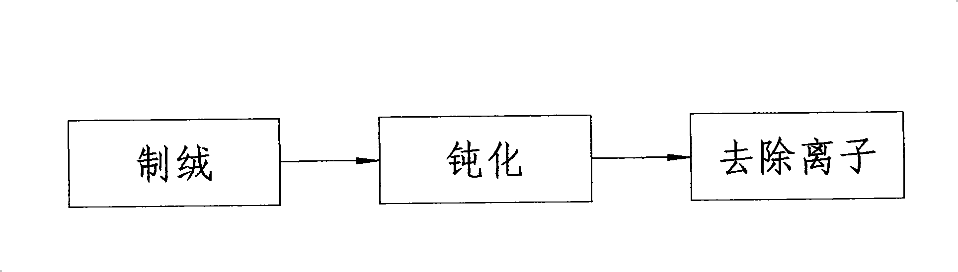
[0021] refer to figure 1 , a method for texturing monocrystalline silicon wafers of the present invention includes corrosion texturing, passivation, and ion removal, wherein: the corrosion texturing is as follows: the single crystal silicon wafers to be texturized after cleaning are placed in a container There are 0.8% by weight of analytically pure sodium hydroxide NaOH, 5.3% of electronic grade isopropanol C 3 h 3 O, 1.4% analytically pure sodium silicate Na 2 SiO 3 9H 2 O, 92.5% pure water H 2 In the texturing tank of the texturing liquid composed of O, under the conditions of 88°C±2°C liquid temperature, one atmospheric pressure, and 0.15MPa nitrogen microbubble stirring, the texturing is etched for 25 to 35 minutes, and formed on the surface of the monocrystalline silicon wafer. The operation process of the textured surface of the microcone structure; the passivation is that the monocrystalline silicon chip after the corrosion making of the texture is placed in a con...


PUM

PropertyMeasurementUnit
reflectanceaaaaaaaaaa

Abstract

The invention discloses a method for texturing a monocrystalline silicon wafer. The method comprises the steps of texturing by corrosion, passivation and deionization. By the technical scheme of cancelling rough polishing, and changing a formula, reaction conditions and treatment flow, the method overcomes the problems and the disadvantages of the prior art that the texturing technological process is difficult to be controlled, the thickness reduction of the monocrystalline silicon wafer is greater, the silicon wafer is easily cracked during the treatment process, the textures formed on the silicon wafer is uneven, and bulky dimension of a cone structure leads to high reflectivity of the silicon wafer, lower short circuit current (Isc) and lower photoelectric conversion rate. The method provided for texturing the monocrystalline silicon wafer realizes that corrosive liquid is in a steady state which is easy to be controlled, the thickness reduction of the silicon wafer is reduced, the formed textures are even and the dimension of the cone structure is compact; the method reaches the purposes of reducing the reflectivity of the silicon wafer, increasing the short circuit current (Isc), and improving the photoelectric conversion rate, meanwhile, the method improves the quality and the qualification rate of the product on the whole, reduces the consumption of chemical reagents and lowers the cost.

Description

technical field [0001] The invention relates to a manufacturing process of a solar cell, in particular to a method for making texture of a monocrystalline silicon chip applied in the texturing process in the manufacturing process of a single crystal silicon solar cell. Background technique [0002] The texturing of solar cells is to produce anisotropic corrosion on the surface of silicon wafers through chemical reactions to form dense micro-pyramidal textured surfaces, so that solar cells can minimize light reflectivity and improve short-circuit resistance. Current (Isc), that is, to increase the photoelectric conversion efficiency. [0003] The processing flow of the prior art texturing process is rough throwing, texturing, passivation, and ion removal. Its formula, reaction condition are: [0004] Coarse throwing: weight percentage, sodium hydroxide NaOH, 7%, pure water H 2 O, 93%, temperature 86℃±2℃, time 2~3min; [0005] Texturing: weight percent, sodium hydroxide Na...

Claims


Application Information

Patent Timeline
Patent Type & Authority Applications(China)
IPC IPC(8): H01L31/18
CPCY02P70/50
Inventor 林海峰
Owner SHANGHAI CHAORI (LUOYANG) SOLAR ENERGY CO LTD
Why Eureka
Try Eureka