Array substrate, manufacturing method thereof and display device
A technology of an array substrate and a manufacturing method, which is applied in the display field and can solve problems such as the inability to realize borderless display and the like
- Summary
- Abstract
- Description
- Claims
- Application Information
AI Technical Summary
Problems solved by technology
Method used
Image

Examples
Embodiment 1
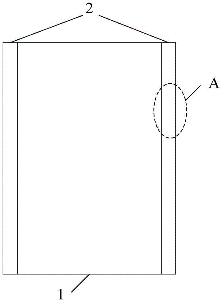
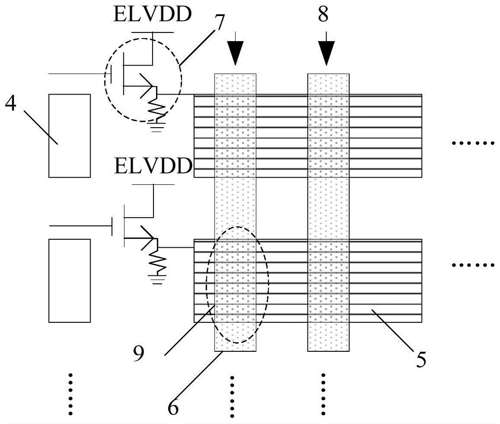
[0053] This embodiment provides an array substrate, including a display area and a gate electrode driving GOA circuit area outside the display area, wherein a passive matrix organic light emitting diode (PMOLED) display array is formed in the GOA circuit area.
[0054] For AMOLED display, each AMOLED display unit needs to be driven by a corresponding TFT (Thin Film Transistor), and there are many traces in the GOA circuit area of the array substrate, and a TFT array cannot be formed in the GOA circuit area, so in the GOA area It is impossible to form an AMOLED display array; and for PMOLED display, each row of PMOLED display units is driven by a gate TFT. Taking advantage of this, this embodiment forms a PMOLED display array in the GOA circuit area, and the AMOLED display unit in the display area is connected. Connect and display images together, so that display can also be performed in the GOA circuit area, so as to realize narrow frame or no frame of the display device.
...
Embodiment 2
[0060] This embodiment provides a display device, including the above-mentioned array substrate. The display device may be any product or component with a display function such as a display panel, a television, a monitor, a digital photo frame, a mobile phone, a tablet computer, and the like.
Embodiment 3
[0062] This embodiment provides a method for manufacturing an array substrate. The array substrate includes a display area and a gate electrode driving GOA circuit area outside the display area. The manufacturing method includes:
[0063] A passive matrix organic light emitting diode PMOLED display array is formed in the GOA circuit area.
[0064] For AMOLED display, each AMOLED display unit needs to be driven by a corresponding TFT, and there are many traces in the GOA circuit area of the array substrate, and the TFT array cannot be formed in the GOA circuit area, so AMOLED display cannot be formed in the GOA area. For PMOLED display, each row of PMOLED display units is driven by a gate TFT. Taking advantage of this, this embodiment forms a PMOLED display array in the GOA circuit area, and connects with the AMOLED display units in the display area to jointly display In this way, it can also be displayed in the GOA circuit area, so as to realize the narrow frame or no frame ...
PUM
| Property | Measurement | Unit |
|---|---|---|
| Thickness | aaaaa | aaaaa |
Abstract
Description
Claims
Application Information