A method for obtaining full-color-spectrum structural color through preparing metal holes having a chassis by utilizing nano-imprint lithography

A nano-imprinting and structural color technology, applied in the field of material technology and nano-processing, can solve problems such as being unsuitable for industrial production, difficult, and inefficient.

Inactive Publication Date: 2015-09-16
FUDAN UNIV
View PDF4 Cites 7 Cited by
  • Summary
  • Abstract
  • Description
  • Claims
  • Application Information

AI Technical Summary

Problems solved by technology

[0004] The artificial preparation of the above structures usually includes methods such as coating, self-assembly, electron beam lithography, laser interference exposure, etc., which are relatively difficult, costly but inefficient, and are not suitable for industrial production.

Method used


Image

  • A method for obtaining full-color-spectrum structural color through preparing metal holes having a chassis by utilizing nano-imprint lithography
  • A method for obtaining full-color-spectrum structural color through preparing metal holes having a chassis by utilizing nano-imprint lithography
  • A method for obtaining full-color-spectrum structural color through preparing metal holes having a chassis by utilizing nano-imprint lithography

Examples


Embodiment 1

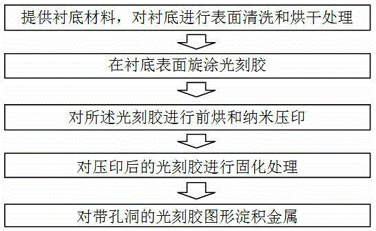
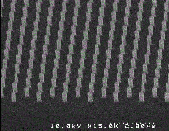
[0028] In this exemplary embodiment: use quartz as the substrate, the PMMA photoresist is a nanoimprint photoresist, and the selected nanostructure is a series of square-arranged hole patterns with different diameters / periods, and the size is represented by a diameter of 10 nanometers / period. Period 20nm is variable 100nm / 200nm, 110nm / 220nm, ..., 250nm / 500nm:

[0029] (1) Routinely clean the quartz plate substrate material, and place it on a 150 hot plate for 5 minutes to dry;

[0030] (2) Spin-coat PMMA photoresist on the surface of the silicon substrate at a spin speed of 1500 rpm for 60 seconds to obtain a photoresist with a thickness of 200 nanometers;

[0031] (3) Pre-baking the spin-coated PMMA photoresist in an oven at a temperature of 180 degrees Celsius for 60 seconds; The printing pressure is 80bar, and the printing time is 5 minutes;

[0032] (4) No special photoresist curing treatment is required for PMMA photoresist;

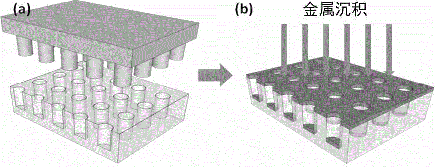
[0033] (5) Perform thermal evaporation of ...

Embodiment 2

[0035] In this exemplary embodiment: use quartz as the substrate, the SU-8 photoresist is a nanoimprint photoresist, and the selected nanostructures are a series of square-arranged hole patterns with different diameters / periods, and the size is represented by a diameter of 10 nm / period 20nm as variable 100nm / 200nm, 110nm / 220nm, ..., 250nm / 500nm:

[0036] (1) Routinely clean the quartz plate substrate material, and place it on a 150 hot plate for 5 minutes to dry;

[0037] (2) Spin-coat SU-8 2000.5 photoresist on the surface of the silicon substrate at a spin speed of 3000 rpm for 60 seconds to obtain a photoresist with a thickness of 500 nm;

[0038] (3) Pre-baking the spin-coated PMMA photoresist in an oven at a temperature of 150 degrees Celsius for 60 seconds; The printing pressure is 50bar, and the printing time is 5 minutes;

[0039] (4) Perform UV curing on the imprinted SU-8 photoresist for 5 minutes;

[0040] (5) Perform thermal evaporation of the aluminum metal fil...


PUM

PropertyMeasurementUnit
thicknessaaaaaaaaaa
thicknessaaaaaaaaaa

Abstract

The invention belongs to the technical field of material technology and nanofabrication technology and specifically discloses a method for obtaining full-color-spectrum structural color through preparing metal holes having a chassis by utilizing nano-imprint lithography. The method comprises the following steps: carrying out cleaning and drying treatment on the surface of a substrate; carrying out substrate photoresist spin coating and pre-baking; carrying out nano-imprinting on the photoresist; carrying out ultraviolet light solidification processing on the photoresist obtained after the nano-imprinting; and depositing metal on the photoresist obtained after the nano-imprinting and the like. A metal hole array having the chassis obtained through the method has abnormal transmitting spectrum peak which is adjustable in peak position in a visible light waveband (360-810 nm), and the reflected single-color structural color in full color spectrum can be used for a CCD color filter or a color display and the like.

Description

technical field [0001] The invention belongs to the field of material technology and nano-processing technology, and specifically relates to a method for preparing metal holes with a chassis by using nano-imprinting to obtain full-chromatographic structural color. Background technique [0002] Structural color, also known as physical color, is an optical effect caused by the submicroscopic physical structure of the material itself, which has nothing to do with pigment coloring. Structural color presents a specific color through the selective reflection and transmission of visible light through the microstructure of the material. It has the characteristics of high brightness, high saturation, non-fading, iridescence, and polarization effects. It has a wide range of applications in display, decoration, and anti-counterfeiting. prospect. [0003] Structural color originates from the interaction between natural light and microstructures. The color formation mainly includes phys...

Claims


Application Information

Patent Timeline
Patent Type & Authority Applications(China)
IPC IPC(8): G02B5/20G03F7/00
CPCG02B5/20G03F7/0002
Inventor 陆冰睿陈宜方马亚琪张思超
Owner FUDAN UNIV
Why Eureka
Try Eureka