
Eureka
For R&D, Eureka makes reading and utilizing patents & technical documents easy.
Eureka AIR
Designed for self-driven R&D workflows. Generate viable solutions, solve complex R&D challenges, empower your innovation with AI.

Eureka Materials
Designed for material experts only. Revolutionize your material R&D, from search, analyze, to developing new materials.

TechResearch
Generate reliable direction feasibility study reports for your R&D in just a few steps.

TechSeek
Discover and master advanced knowledge NOW. Basics, ideas, possibilities, all at once.

TechMind
As an expert in R&D Theories, TechMind can generates customized viable solutions instantly.

TechRisk
Analyze your overall solution with one click, know your potential R&D risks in advance.

TechMonitor
Get weekly tech updates, stay abreast of the latest tech innovations and key insights.
Optical film manufacturing method and manufacturing device
A manufacturing method and technology of optical film, applied in optics, optical elements, nonlinear optics, etc., can solve the problems of complex process and high cost of optical film, and achieve the effects of simple operation, less defects, and high production efficiency
- Summary
- Abstract
- Description
- Claims
- Application Information
AI Technical Summary
Problems solved by technology
Method used
Image

Examples
Embodiment 1
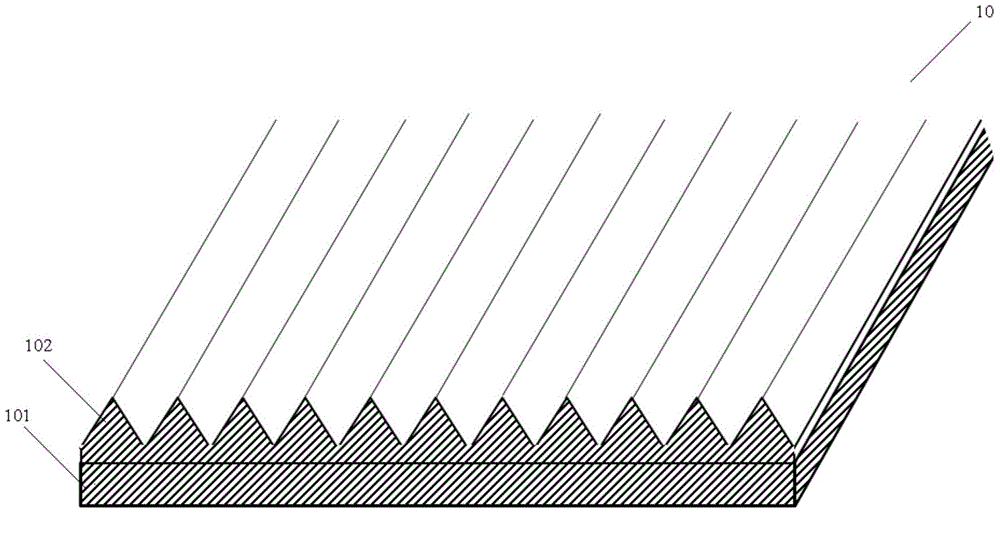
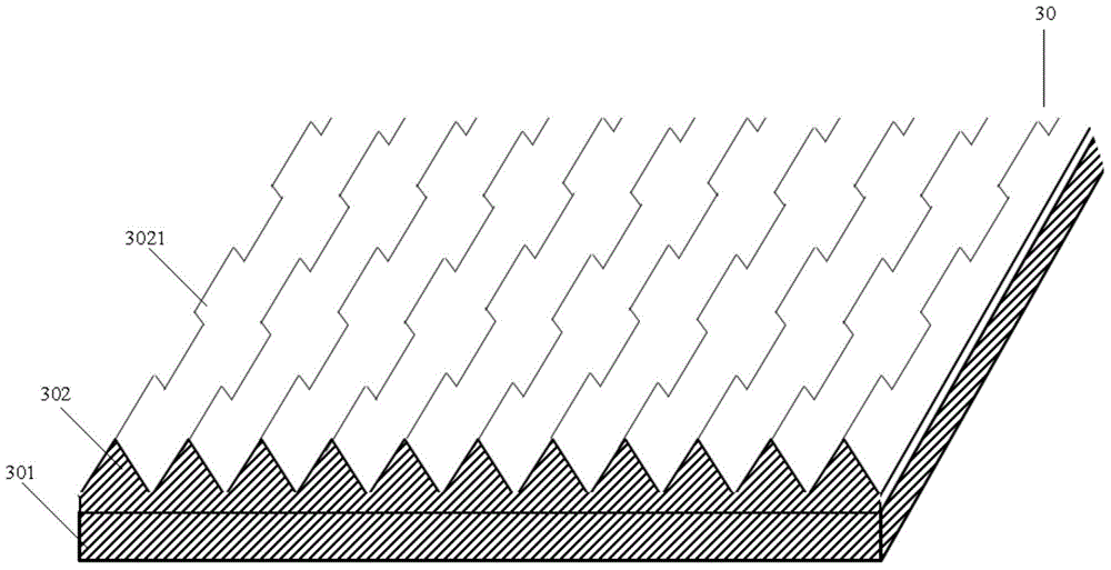
[0028] The invention provides a method for making an optical film. By irradiating ultraviolet light through a substrate with microstructures or patterns on the surface to the ultraviolet light curing glue on the surface of the prism structure of the optical film, the surface formed on the surface of the prism structure is obtained. The corresponding microstructure or pattern of the optical film. The main principle of this scheme is: irradiate the ultraviolet light curing adhesive on the surface of the optical film through the substrate with a microstructure or pattern on the surface, so that the surface of the corresponding microstructure or pattern is formed on the surface of the ultraviolet light curing adhesive. The intensity of ultraviolet light behind the surface of the substrate with microstructure or pattern changes with the structure of its microstructure or pattern, so that the corresponding microstructure or pattern is formed on the surface of the optical film, increa...
Embodiment 2
[0045] This solution also provides an optical film, and the optical film is an optical film obtained by the method for manufacturing an optical film as described in any one of the above embodiments.
[0046] Specifically, the optical film includes a base material and a prism layer, the base material includes a first optical surface and a second optical surface positioned on the first optical surface, and the prism layer is arranged on the first optical surface of the base material. On the optical surface; on the surface opposite to the first optical surface in the prism layer, a microstructure or pattern that can adjust the light-gathering effect of the prism layer is arranged; the microstructure or pattern has a The corresponding microstructure or pattern of the substrate is formed by irradiating the prism layer of the optical film. That is, in this embodiment, microstructures or patterns of various shapes are formed on the surface of the prism layer of the optical film, and ...
Embodiment 3
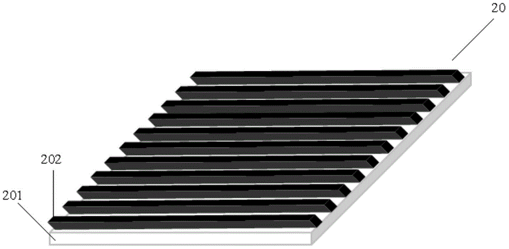
[0052] In this embodiment, for the sake of clarity, the substrate with a microstructure or pattern on the surface is defined as the second substrate, and the substrate of the optical film is defined as the first substrate; mode, there are two types of optical film production equipment, in this embodiment, the two optical film production equipment are respectively the first optical film production equipment and the second optical film production equipment; the first optical film production equipment includes : The first optical film production device, the first optical film production device is used to coat the prism resin on the optical surface of the first substrate, and at the same time transmit the ultraviolet light through the second substrate with microstructure or pattern on the surface The material is irradiated to the prism resin of the first substrate to obtain an optical film having a corresponding microstructure or pattern on the surface. The principle of this schem...
PUM
 Abstract
Description
Claims
Application Information
 - R&D Engineer
- R&D Manager
- IP Professional
- Industry Leading Data Capabilities
- Powerful AI technology
- Patent DNA Extraction
Browse by: Latest US Patents, China's latest patents, Technical Efficacy Thesaurus, Application Domain, Technology Topic, Popular Technical Reports.
© 2024 PatSnap. All rights reserved.Legal|Privacy policy|Modern Slavery Act Transparency Statement|Sitemap|About US| Contact US: help@patsnap.com