
Integrated touch amoled display device and preparation method thereof

A display device and touch screen sensor technology, applied in the field of semiconductor device preparation, can solve problems such as heavy weight, high cost, parallax, etc., and achieve the effects of eliminating parallax problems, reducing manufacturing costs, and reducing device thickness.

Active Publication Date: 2018-03-09
TRULY HUIZHOU SMART DISPLAY
View PDF5 Cites 0 Cited by
  • Summary
  • Abstract
  • Description
  • Claims
  • Application Information

AI Technical Summary

Problems solved by technology

[0004] A touch screen sensor is pasted on the package cover outside the AMOLED, and then the cover glass (Cover Lens) is pasted on the touch screen sensor. Sometimes in order to enhance the strength of the Cover Lens, it is even necessary to use strengthened glass, which causes the display device in the traditional technology. Relatively large thickness, heavy weight, and high cost. At the same time, there is a gap between the AMOLED screen and the touch screen, which will cause technical problems such as reduced readability and parallax.

Method used


Image

  • Integrated touch amoled display device and preparation method thereof
  • Integrated touch amoled display device and preparation method thereof
  • Integrated touch amoled display device and preparation method thereof

Examples


Embodiment Construction

[0042] In order to make the object, technical solution and advantages of the present invention clearer, the present invention will be further described in detail below in conjunction with the accompanying drawings and embodiments. It should be understood that the specific embodiments described here are only used to explain the present invention, not to limit the present invention.

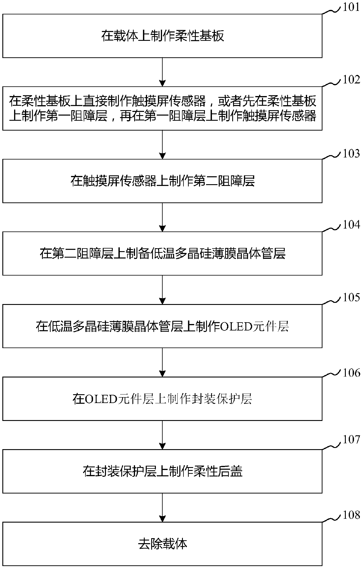
[0043] see figure 1 In one embodiment, a method for manufacturing an integrated touch AMOLED display device is provided, including:

[0044] Step 101, making a flexible substrate on a carrier.

[0045] Specifically, the carrier in this step may be a glass carrier. This step is specifically: coating a PI film (Polymide Film, polyimide film) on a glass carrier, and thermally baking the PI film (for example, heating in nitrogen, 160-280° C. for 3 to 4 hours) to form flexible substrate.

[0046] Step 102 , fabricating a touch screen sensor directly on the flexible substrate, or fabricating a first ...


PUM


Abstract

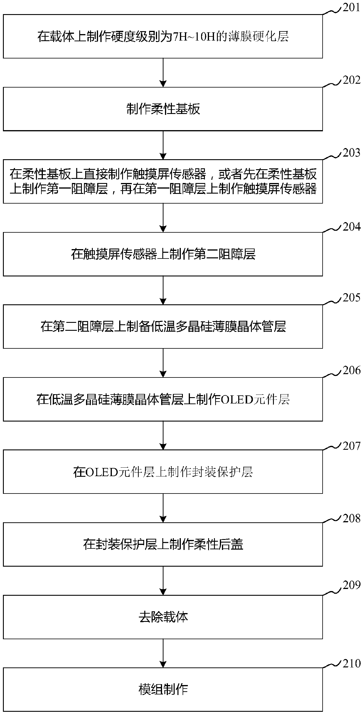
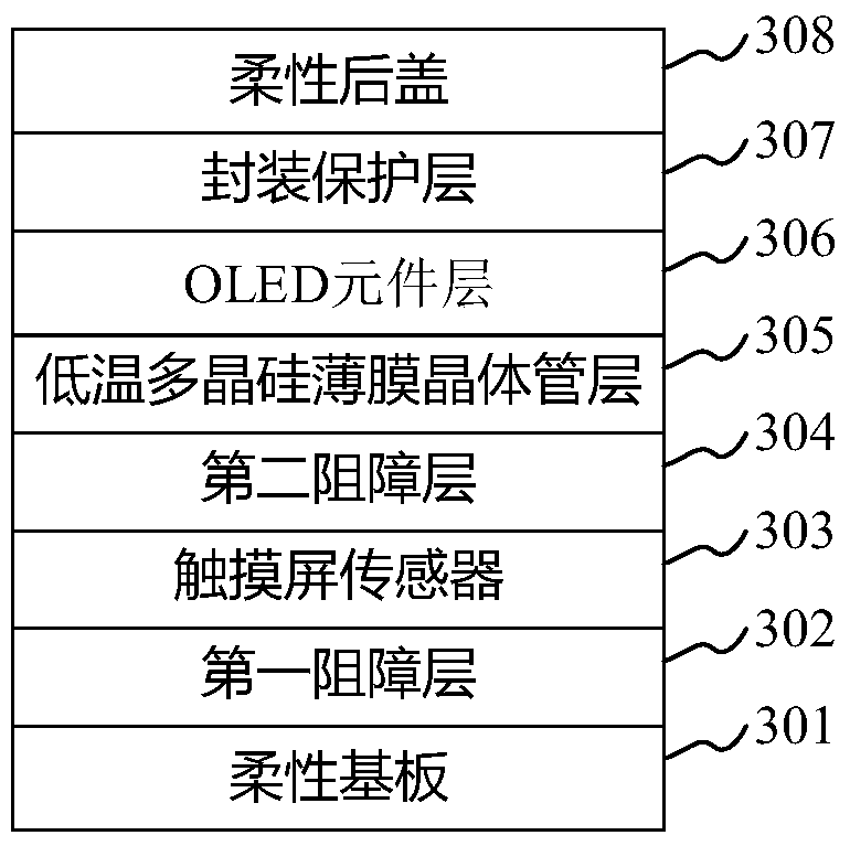
The invention discloses a method for preparing an integrated touch AMOLED display device, comprising: manufacturing a flexible substrate on a carrier; directly manufacturing a touch screen sensor on the flexible substrate, or first manufacturing a first barrier layer on the flexible substrate, Make a touch screen sensor on the first barrier layer; make a second barrier layer on the touch screen sensor; prepare a low-temperature polysilicon thin film transistor layer on the second barrier layer; An OLED element layer is fabricated on the OLED element layer; an encapsulation protective layer is fabricated on the OLED element layer; a flexible back cover is fabricated on the encapsulation protective layer; and the carrier is removed. By applying the technical scheme of the invention, the thickness and cost of the integrated touch AMOLED display device can be reduced, and parallax can be eliminated.

Description

technical field [0001] The invention relates to the technical field of semiconductor device preparation, in particular to an integrated touch AMOLED display device and a preparation method thereof. Background technique [0002] AMOLED (Active Matrix Organic Light Emitting Diode, Active Matrix Organic Light Emitting Diode) is recognized as a new generation of display panels. Compared with ordinary liquid crystal panels, it has the technical advantages of faster response speed, higher contrast ratio, and wider viewing angle. [0003] With the advancement of AMOLED technology, the application scenarios of AMOLED are becoming more and more extensive. For example, AMOLED displays are also used in smart mobile display terminals. Usually, smart mobile display terminals also need to integrate touch screen technology in order to facilitate the use and operation of users. Therefore, it is necessary to combine AMOLED display technology and touch technology in smart mobile display termi...

Claims


Application Information

Patent Timeline
Patent Type & Authority Patents(China)
IPC IPC(8): H01L51/56H01L27/32
CPCH10K59/40H10K71/00
Inventor 苏君海谢志生宋小进李建华
Owner TRULY HUIZHOU SMART DISPLAY
Learn More