Eureka AIR delivers breakthrough ideas for toughest innovation challenges, trusted by R&D personnel around the world.

Integrated touch-control transparent AMOLED display device and preparation method thereof

A display device, transparent technology, applied in semiconductor/solid-state device manufacturing, electric solid-state devices, semiconductor devices, etc., can solve problems such as high cost, heavy weight, parallax, etc., to reduce device thickness, eliminate parallax problems, and reduce manufacturing costs Effect

Active Publication Date: 2015-08-19
TRULY HUIZHOU SMART DISPLAY
View PDF4 Cites 12 Cited by
  • Summary
  • Abstract
  • Description
  • Claims
  • Application Information

AI Technical Summary

Problems solved by technology

In the traditional technology, the touch screen sensor is pasted on the package cover outside the transparent AMOLED, and then the cover glass (Cover Lens) is pasted on the touch screen sensor. Sometimes in order to enhance the strength of the Cover Lens, it is even necessary to use strengthened glass, which is As a result, the overall thickness of the display device in the traditional technology is relatively large, the weight is large, and the cost is high. At the same time, there is a gap between the AMOLED screen and the touch screen, which will cause technical problems such as reduced readability and parallax.

Method used


Image

  • Integrated touch-control transparent AMOLED display device and preparation method thereof

Examples


Embodiment Construction

[0042] In order to make the object, technical solution and advantages of the present invention clearer, the present invention will be further described in detail below in conjunction with the accompanying drawings and embodiments. It should be understood that the specific embodiments described here are only used to explain the present invention, not to limit the present invention.

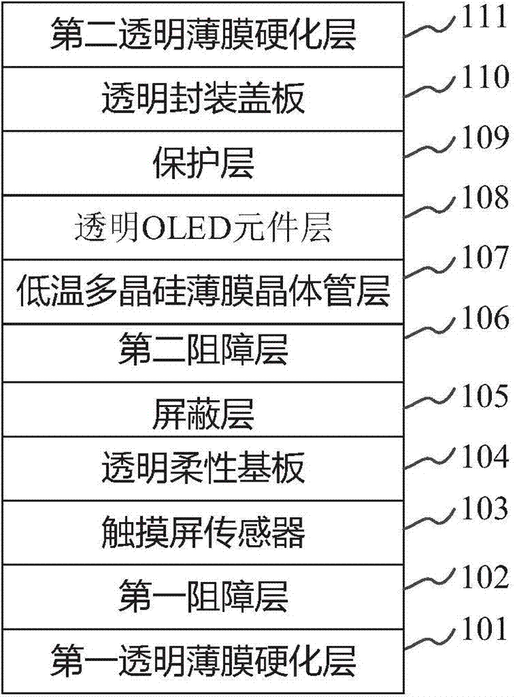
[0043] see figure 1 , an integrated touch transparent AMOLED display device is provided in one embodiment, comprising:

[0044] The first transparent film hardening layer 101;

[0045] a first barrier layer 102 on the first transparent thin film hardening layer 101;

[0046] a touch screen sensor 103 on the first barrier layer 102;

[0047] a transparent flexible substrate 104 on the touch screen sensor 103;

[0048] shielding layer 105 and second barrier layer 106 on the transparent flexible substrate 104;

[0049] A low temperature polysilicon thin film transistor layer 107 on the second bar...


PUM

PropertyMeasurementUnit
Hardnessaaaaaaaaaa

Abstract

The invention discloses a preparation method of an integrated touch-control transparent active matrix organic light emitting diode (AMOLED) display device. The preparation method comprises: manufacturing a buffer layer on a carrier; manufacturing a first transparent thin-film hardening layer on the buffer layer; manufacturing a first barrier layer on the first transparent thin-film hardening layer; manufacturing a touch screen sensor on the first barrier layer; manufacturing a transparent flexible substrate on the touch screen sensor; manufacturing a shielding layer and a second barrier layer on the transparent flexible substrate; preparing a low-temperature polycrystalline thin-film transistor layer on the second barrier layer; manufacturing a transparent OLED element layer on the low-temperature polycrystalline thin-film transistor layer; manufacturing a protection layer on the transparent OLED element layer; manufacturing a transparent packaging cover plate on the protection layer; manufacturing a second transparent thin-film hardening layer on the transparent packaging cover plate; and removing the carrier and the buffer layer. On the basis of the technical scheme, the thickness and cost of the integrated touch-control transparent AMOLED display device can be reduced and the parallax can be eliminated.

Description

technical field [0001] The invention relates to the technical field of semiconductor device preparation, in particular to an integrated touch-sensitive transparent AMOLED display device and a preparation method thereof. Background technique [0002] AMOLED (Active Matrix Organic Light Emitting Diode, Active Matrix Organic Light Emitting Diode) is recognized as a new generation of display panels. Compared with ordinary liquid crystal panels, it has the technical advantages of faster response speed, higher contrast ratio, and wider viewing angle. [0003] With the advancement of AMOLED technology, the application scenarios of AMOLED are becoming more and more extensive, and the transparency of AMOLED display devices has always been a market demand. In addition, in order to facilitate the use and operation of users, display devices also need to integrate touch screen technology. Therefore, in the field of display technology, it is necessary to combine transparent AMOLED display...

Claims


Application Information

Patent Timeline
IPC IPC(8): H01L27/32H01L21/77
Inventor 苏君海谢志生宋小进李建华
Owner TRULY HUIZHOU SMART DISPLAY
Why Eureka
Eureka Blog
Learn More