Wafer processing method

Active Publication Date: 2009-01-15
DISCO CORP
View PDF6 Cites 9 Cited by
  • Summary
  • Abstract
  • Description
  • Claims
  • Application Information

AI Technical Summary

Benefits of technology

[0007]It is therefore an object of the present invention to provide a wafer processing method which can facilitate handling of a thin wafer to be separated into indivi

Problems solved by technology

In the case that the electrodes of the interposer and the semiconductor chip are connected by wire bonding, there is a possibility that the gold wires connecting the electrodes may be deformed in the resin molding step, causing a break or short circuit.
In some case, the air remaining in the molding resin may be expanded in heating to cause damage to the semiconductor chip.
Further, since the semiconductor chip is stacked on the interposer in the condition where the front side

Method used


Image

  • Wafer processing method
  • Wafer processing method
  • Wafer processing method

Examples


Embodiment Construction

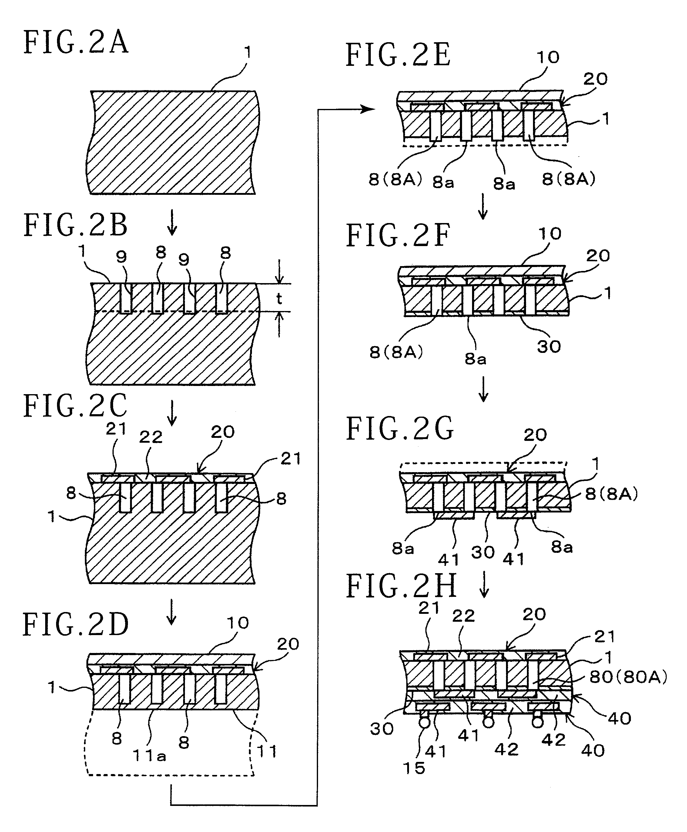
[0025]A preferred embodiment of the present invention will now be described with reference to the drawings.

[1] Semiconductor Wafer

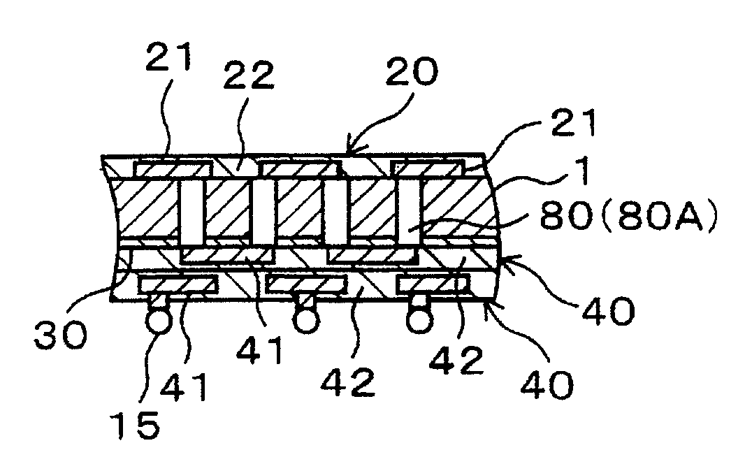
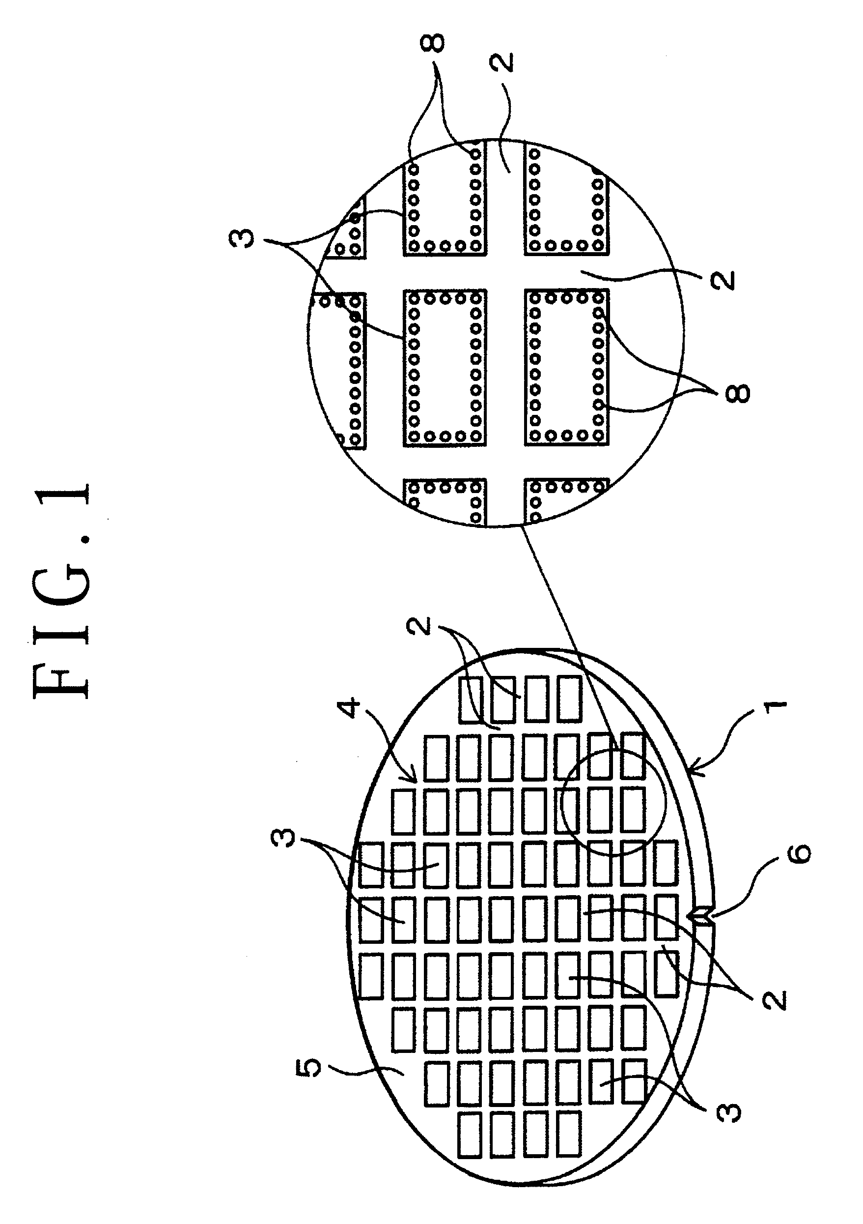
[0026]Reference numeral 1 shown in FIG. 1 denotes a disk-shaped semiconductor wafer as a substrate to be processed into semiconductor chips. The wafer 1 is a silicon wafer, for example, and the thickness of the wafer 1 is about 600 μm, for example. A plurality of crossing streets 2 are formed on the front side of the wafer 1 to thereby partition a plurality of rectangular semiconductor chips (devices) 3. An electronic circuit such as IC or LSI (not shown) is formed on the front side of each semiconductor chip 3.

[0027]These plural semiconductor chips 3 are formed in a generally circular device forming area 4 concentric with the wafer 1. The device forming area 4 occupies a large part of the wafer 1. The remaining peripheral portion of the wafer 1 around the device forming area 4 is formed as an annular remaining peripheral area 5 where the semiconductor ch...


PUM


Abstract

A wafer processing method having a step of reducing the thickness of a wafer in only a device forming area where semiconductor chips are formed by grinding and etching the back side of the wafer to thereby form a recess on the back side of the wafer. At the same time, an annular projection is formed around the recess to thereby ensure the rigidity of the wafer. Accordingly, handling in shifting the wafer from the back side recess forming step to a subsequent step of forming a back side rewiring layer can be performed safely and easily.

Description

BACKGROUND OF THE INVENTION[0001]1. Field of the Invention[0002]The present invention relates to a method of processing a wafer to obtain a plurality of devices such as semiconductor chips having through metal electrodes, and more particularly to a technique of forming a rewiring layer on the back side of the wafer.[0003]2. Description of the Related Art[0004]In recent semiconductor device technologies, a semiconductor package having substantially the same size as that of a semiconductor chip called a CSP (Chip Size Package) is effectively used in achieving an increase in packaging density and a reduction in size and thickness. A conventional manufacturing method for such a semiconductor package includes the steps of stacking a semiconductor chip on a package substrate called an interposer, electrically connecting electrodes of the interposer and the semiconductor chip through gold wires by wire bonding, and molding the semiconductor chip and the interposer with resin. There is a ca...

Claims


Application Information

Patent Timeline
IPC IPC(8): H01L21/768
CPCH01L21/304H01L2224/05569H01L21/76898H01L21/78H01L24/11H01L24/13H01L24/94H01L2221/6834H01L2221/68372H01L2224/94H01L2924/01078H01L2924/01079H01L2924/19042H01L21/6836H01L2224/131H01L2924/00014H01L2924/10253H01L2224/45124H01L2224/0401H01L2224/45144H01L2924/0002H01L2224/03H01L2224/11H01L2924/00H01L2224/48H01L2924/014H01L2224/05552
Inventor KAJIYAMA, KEIICHIARAI, KAZUHISA
Owner DISCO CORP
Why Eureka
Try Eureka