Method for Manufacturing a Semiconductor Wafer, and Semiconductor Device Having a Low Concentration of Interstitial Oxygen

a technology of interstitial oxygen and manufacturing method, which is applied in the direction of semiconductor devices, semiconductor/solid-state device details, electrical apparatus, etc., can solve the problems of insufficiently low concentration of interstitial oxygen, fz processes are more expensive than cz processes, and the size of ingots which can be produced by fz processes is limited to about 200 mm in diameter, so as to reduce the oxygen content reduce the thickness of the device wafer

Active Publication Date: 2016-04-14
INFINEON TECH AG
View PDF4 Cites 10 Cited by
  • Summary
  • Abstract
  • Description
  • Claims
  • Application Information

AI Technical Summary

Benefits of technology

[0008]According to an embodiment, a method for manufacturing a substrate wafer includes: providing a device wafer having a first side and a second side opposite the first side, the device wafer being made of a semiconductor material and having a first thickness; subjecting the device wafer to a first high temperature process for reducing the oxygen content of the device wafer at least in a region at the second side; bonding the second side of the device wafer to a first side of a carrier wafer to form a substrate wafer comprising the device wafer bonded to the carrier wafer, the carrier wafer having a second side opposite the first side which second side of the carrier wafer forms the second side of the substrate wafer, wherein the first side of the device wafer forms a first side of the substrate wafer; processing the first side of the substrate wafer, which is formed by the first side of the device wafer, to reduce the thickness of the device wafer to a second thickness which is less than the first thickness of the device wafer; subjecting the substrate wafer to a second high temperature process for reducing the oxygen content at least of the device wafer bonded to the carrier wafer; and at least partially integrating at least one semiconductor component into the device wafer after the second high temperature process.

Problems solved by technology

However, the size of the ingots which can be produced by FZ processes is limited to about 200 mm in diameter.
Furthermore, FZ processes are more expensive than CZ processes.
FZ processes allow the manufacturing of ingots having a sufficiently low concentration of interstitial oxygen at high cost.
Such a variation is too large for many semiconductor devices, particularly power devices, so that a large portion of the ingots cannot be used for the intended purpose.
This further increases the manufacturing costs.

Method used


Image

  • Method for Manufacturing a Semiconductor Wafer, and Semiconductor Device Having a Low Concentration of Interstitial Oxygen
  • Method for Manufacturing a Semiconductor Wafer, and Semiconductor Device Having a Low Concentration of Interstitial Oxygen
  • Method for Manufacturing a Semiconductor Wafer, and Semiconductor Device Having a Low Concentration of Interstitial Oxygen

Examples


Embodiment Construction

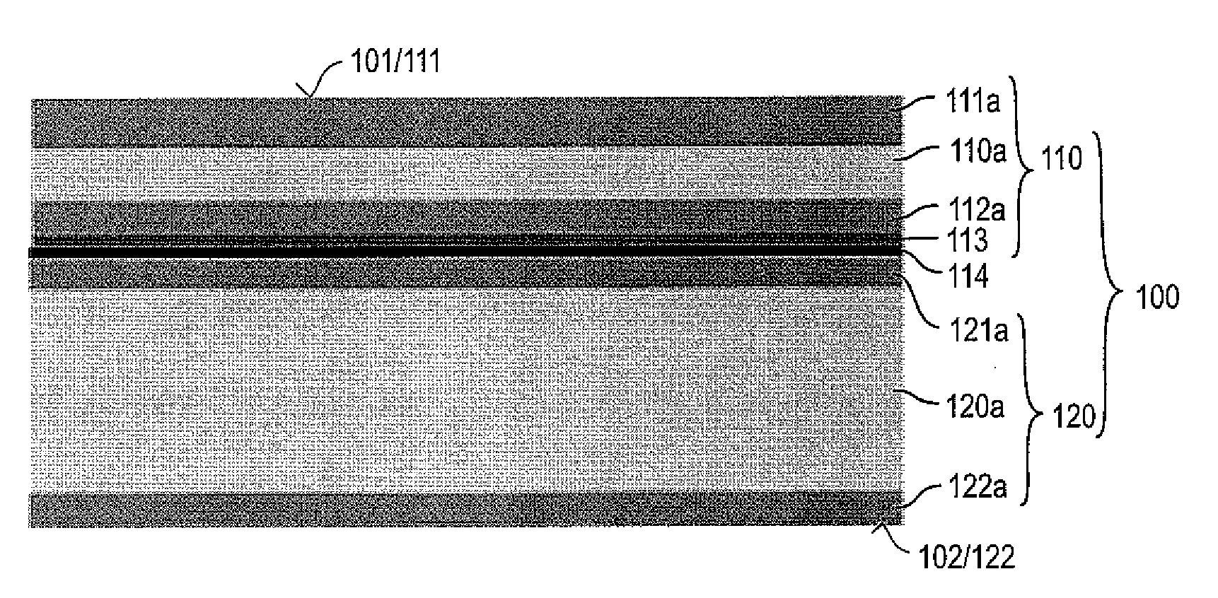
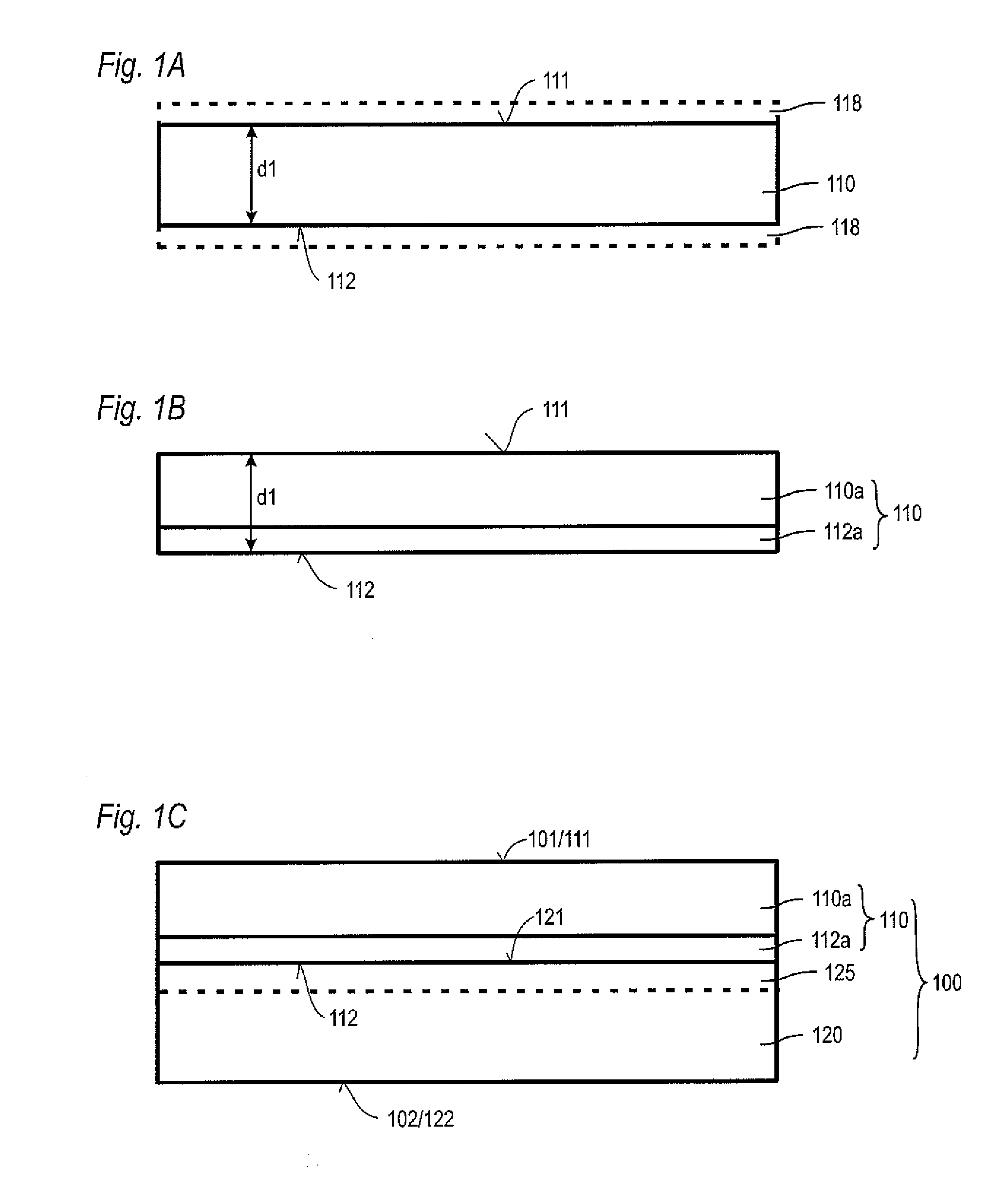
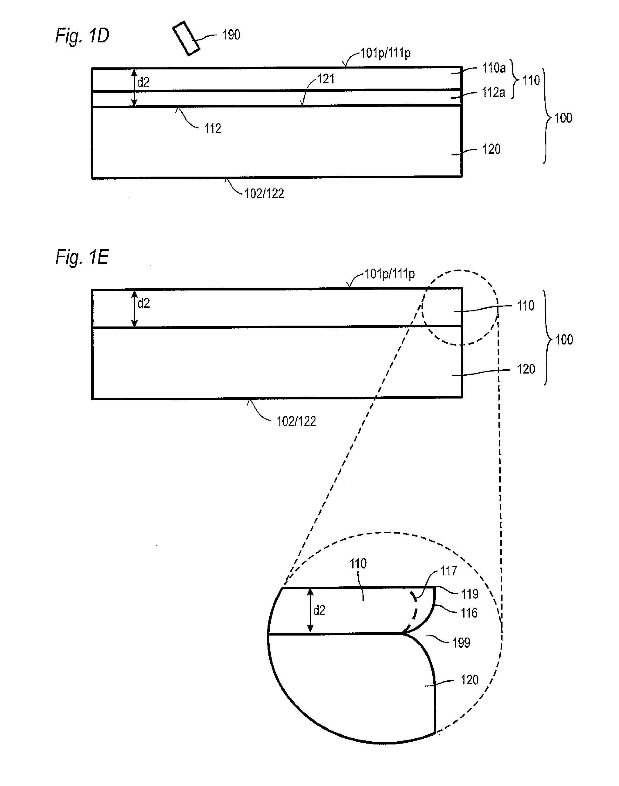
[0021]In the following detailed description, reference is made to the accompanying drawings, which form a part hereof, and in which are shown by way of illustration specific embodiments in which the invention may be practiced. In this regard, directional terminology, such as “top”, “bottom”, “front”, “back”, leading”, “trailing”, “lateral”, “vertical” etc., is used with reference to the orientation of the Figure(s) being described. Because components of embodiments can be positioned in a number of different orientations, the directional terminology is used for purpose of illustration and is in no way limiting. It is to be understood that other embodiments may be utilised and structural or logical changes may be made without departing from the scope of the present invention. The following detailed description, therefore, is not to be taken in a limiting sense, and the scope of the present invention is defined by the appended claims. The embodiments being described use specific langua...


PUM


Abstract

A method for manufacturing a substrate wafer 100 includes providing a device wafer (110) having a first side (111) and a second side (112); subjecting the device wafer (110) to a first high temperature process for reducing the oxygen content of the device wafer (110) at least in a region (112a) at the second side (112); bonding the second side (112) of the device wafer (110) to a first side (121) of a carrier wafer (120) to form a substrate wafer (100); processing the first side (101) of the substrate wafer (100) to reduce the thickness of the device wafer (110); subjecting the substrate wafer (100) to a second high temperature process for reducing the oxygen content at least of the device wafer (110); and at least partially integrating at least one semiconductor component (140) into the device wafer (110) after the second high temperature process.

Description

[0001]The present application claims priority under 35 USC §119 to German (DE) Patent Application Serial No. DE 10 2014 114 683.2 filed on Oct. 9, 2014. The disclosure in this priority application is hereby incorporated fully by reference into the present application.BACKGROUND[0002]1. Technical Field[0003]Embodiments described herein relate to methods for manufacturing semiconductor wafers, and to semiconductor devices having a low concentration of interstitial oxygen. Further embodiments relates to methods for manufacturing semiconductor wafers having a resistivity in a given range.[0004]2. Background Art[0005]Semiconductor devices are processed on semiconductor wafers which are thin plates of cut large semiconductor crystals, which are referred to as ingots. There are basically two different methods to produce semiconductor ingots: methods based on Czochralski process (CZ process) and methods based on the float-zone process (FZ process). The FZ process allows manufacturing of ing...

Claims


Application Information

Patent Timeline
Patent Type & Authority Applications(United States)
IPC IPC(8): H01L21/28H01L21/322
CPCH01L21/3225H01L21/28185H01L21/187H01L21/2257H01L21/268H01L21/28238H01L21/3221H01L21/324H01L21/3242H01L29/66348H01L21/76256H01L29/32H01L29/7813H01L29/66734H01L21/02002H01L29/7397H01L21/02008H01L21/02005H01L21/02016H01L21/0201H01L29/1095H01L29/66325H01L29/7393H01L29/7395
Inventor OEFNER, HELMUTCASPARY, NICOMOMENI, MOHAMMADPLOSS, REINHARDSANTOS RODRIGUEZ, FRANCISCO JAVIERSCHULZE, HANS-JOACHIM
Owner INFINEON TECH AG
Why Eureka
Try Eureka