CMOS fully digital BPSK modulation pulse radio ultra-wideband transmitter

A modulated pulse and radio technology, applied in the ultra-wideband field, can solve the problems of waveform distortion, large chip area and cost, incompatibility of CMOS technology, etc., and achieve the effect of low circuit power consumption, less control signal, and favorable chip integration.

Active Publication Date: 2015-10-07
GUILIN UNIV OF ELECTRONIC TECH
View PDF5 Cites 4 Cited by
  • Summary
  • Abstract
  • Description
  • Claims
  • Application Information

AI Technical Summary

Problems solved by technology

At present, many literatures have been researched on IR-UWB transmitters. These IR-UWB transmitters are mainly realized by the following schemes: Scheme 1 is to use a digital circuit to delay to obtain a narrow pulse. After the narrow pulse passes through the shaping network, the spectrum is moved. To the required frequency band, this scheme needs to use a large number of capacitors, inductors and resistors, so the chip area and cost are large; the second scheme is to use the delay of the digital circuit to generate several narrow pulses, and the

Method used


Image

  • CMOS fully digital BPSK modulation pulse radio ultra-wideband transmitter
  • CMOS fully digital BPSK modulation pulse radio ultra-wideband transmitter
  • CMOS fully digital BPSK modulation pulse radio ultra-wideband transmitter

Examples


Embodiment Construction

[0023] The present invention will be further described below in conjunction with accompanying drawing:

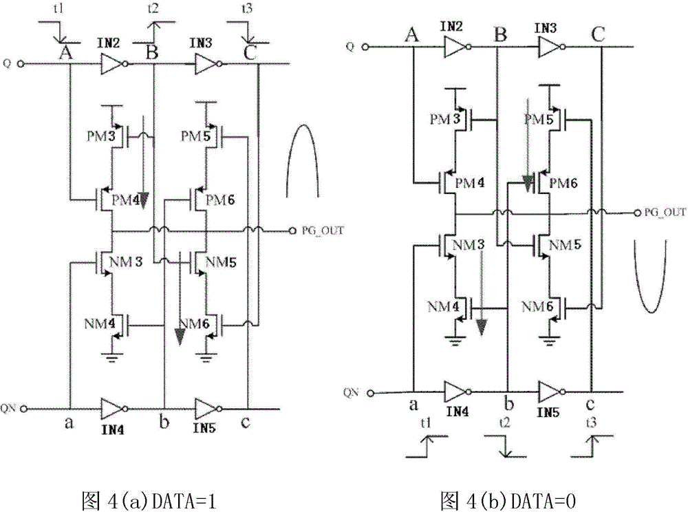
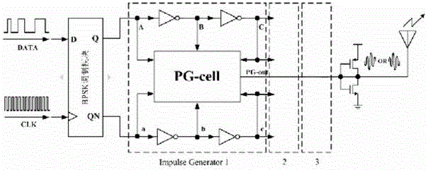
[0024] A CMOS all-digital BPSK modulated pulse radio ultra-wideband transmitter, such as figure 1 As shown, it is mainly composed of BPSK modulation module, delay generation module, pulse sequence generation module, inverter and antenna.

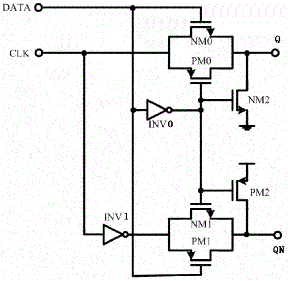
[0025] BPSK modulation modules such as figure 2As shown, it consists of 3 NMOS transistors NM0, NM1, NM2, 3 PMOS transistors PM0, PM1, PM2 and 2 inverters INV0, INV1 circuits. The gate of the NMOS transistor NM0 and the gate of the PMOS transistor PM1 are connected to the input terminal of the inverter INV0 to form the digital signal DATA input terminal of the BPSK modulation module. The gate of the NMOS transistor NM0 and the gate of the PMOS transistor PM1 are connected to the input terminal of the inverter INV0 to form the digital signal DATA input terminal of the BPSK modulation module. The drain of the NMOS transistor NM0, the so...


PUM


Abstract

The invention discloses a CMOS fully digital BPSK modulation pulse radio ultra-wideband transmitter, which includes a BPSK modulation module, a time-delay generation module, a pulse sequence generation module and an antenna. The BPSK modulation module processes an input digital signal DATA and a clock signal CLK, and generates a digital signal that meets BPSK modulation requirements. Each time-delay generation circuit of the time-delay generation module delays a modulation signal output from the BPSK modulation module on the basis of the time-delay characteristics of an inverter and then obtains different time delay outputs, and is used for controlling a corresponding pulse sequence generation circuit so that the pulse sequence generation circuit generates a pulse unit identical in time width. Each pulse sequence generation circuit of the pulse sequence generation module generates a monopulse signal, and all pulse signals are combined to form a pulse sequence, which is output by serving as an output signal and emitted by the antenna. Wireless emission signals generated by the transmitter meet the requirements of the frequency spectrum and the work frequency range of UWB.

Description

technical field [0001] The invention relates to the field of ultra-wideband technology, in particular to a CMOS all-digital BPSK modulated pulse radio ultra-wideband transmitter. Background technique [0002] Since the U.S. Federal Communications Commission (FCC) promulgated the Ultra-Wideband (UWB) spectrum specification in 2002, and used the 3.1GHz-10.6GHz frequency band as an unlicensed frequency band for civilian UWB equipment, Ultra-Wideband Broadband communication technology has been applied research and attention in fields such as wireless personal area network, wireless sensor network, and biomedicine because of its simple system structure, high transmission rate, and low power consumption. [0003] Current UWB communication systems can be divided into three categories: Direct Sequence Spread Spectrum (DS-SS), Multiband Orthogonal Frequency Division Multiplexing (MB-OFDM), and Impulse Radio (IR). Among them, IR-UWB (pulse radio ultra-wideband) technology mainly uses...

Claims


Application Information

Patent Timeline
IPC IPC(8): H04B1/7176H04B1/7163H04B1/40
Inventor 韦保林陈田韦雪明徐卫林段吉海
Owner GUILIN UNIV OF ELECTRONIC TECH
Why Eureka
Try Eureka