
A Compact Time-to-Analog Conversion Circuit for Single Photon Detectors

A single-photon detector and analog conversion technology, applied in the field of single-photon detection, can solve the problems of large layout area and low pixel unit filling factor, and achieve the effects of increasing the detection area, reducing the layout area and reducing power consumption

Active Publication Date: 2020-06-12
NANJING UNIV OF POSTS & TELECOMM
View PDF5 Cites 0 Cited by
  • Summary
  • Abstract
  • Description
  • Claims
  • Application Information

AI Technical Summary

Problems solved by technology

[0005] Purpose of the invention: Aiming at the problems of large layout area and low filling factor of pixel units in the traditional capacitance-integrating TAC circuit, the present invention proposes a compact time-to-analog conversion circuit with high filling factor and high circuit density applied to single photon detectors

Method used


Image

  • A Compact Time-to-Analog Conversion Circuit for Single Photon Detectors
  • A Compact Time-to-Analog Conversion Circuit for Single Photon Detectors
  • A Compact Time-to-Analog Conversion Circuit for Single Photon Detectors

Examples


specific Embodiment

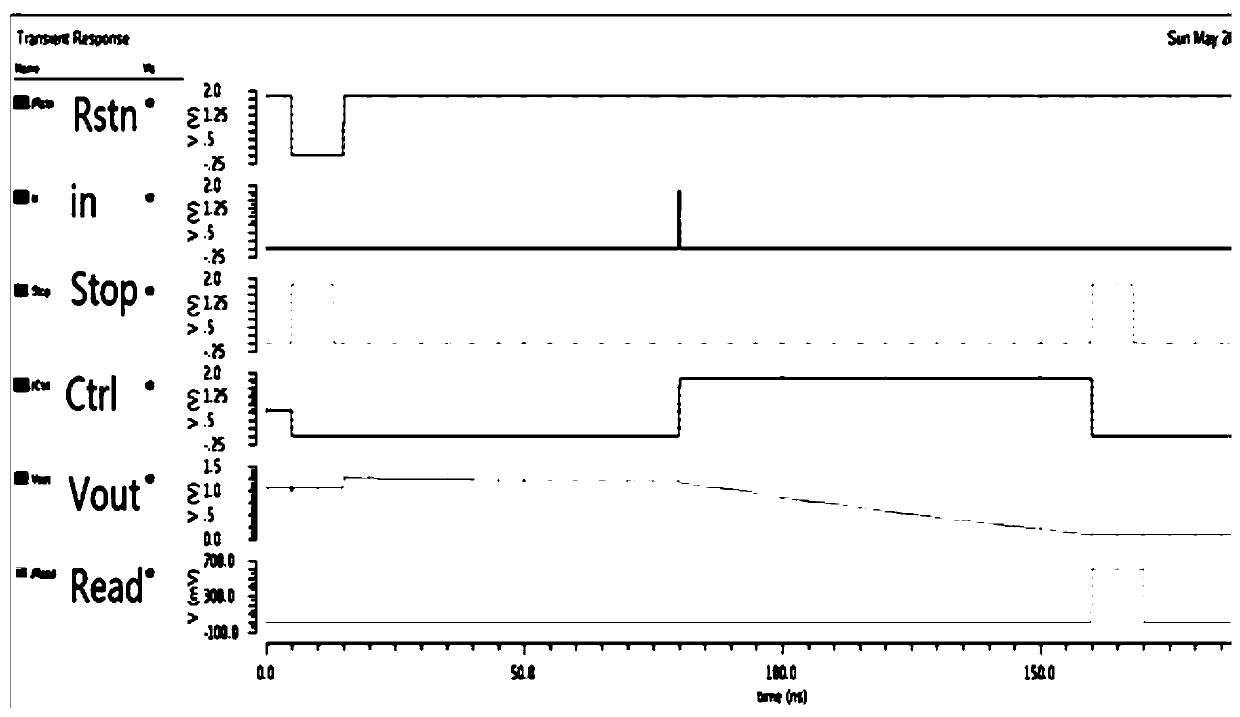
[0039] The present invention simulates the above-mentioned linear time-analog conversion circuit based on capacitor discharge based on a standard 0.18 μm CMOS process. The simulation parameters are as follows: the timing capacitor C is 80fF, and the avalanche pulse input signal is set to a continuous section of pulse width of 200ps. square wave; based on the above simulation parameters, the present invention has carried out the simulation of duration 80ns, and obtains such as image 3 The simulation results shown in Fig. The abscissa in the figure is the simulation time, and the ordinate is the voltage value at the output terminal.

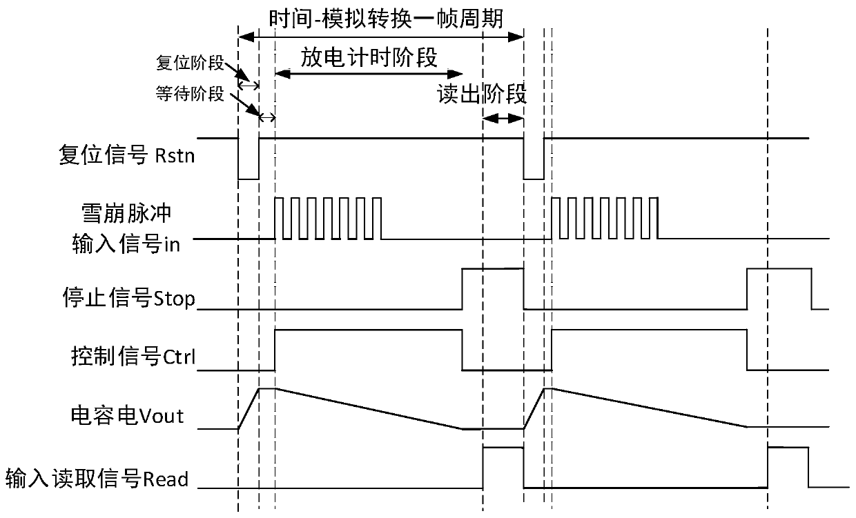
[0040] In the initial stage, due to the MOS voltage division, the timing capacitor C is charged to 1.2V by the reset signal; then the circuit detects the first avalanche pulse signal, which is triggered by the avalanche pulse input signal in and the input stop signal Stop to make the control logic signal Ctrl and its The reverse signal Ctrln chan...


PUM


Abstract

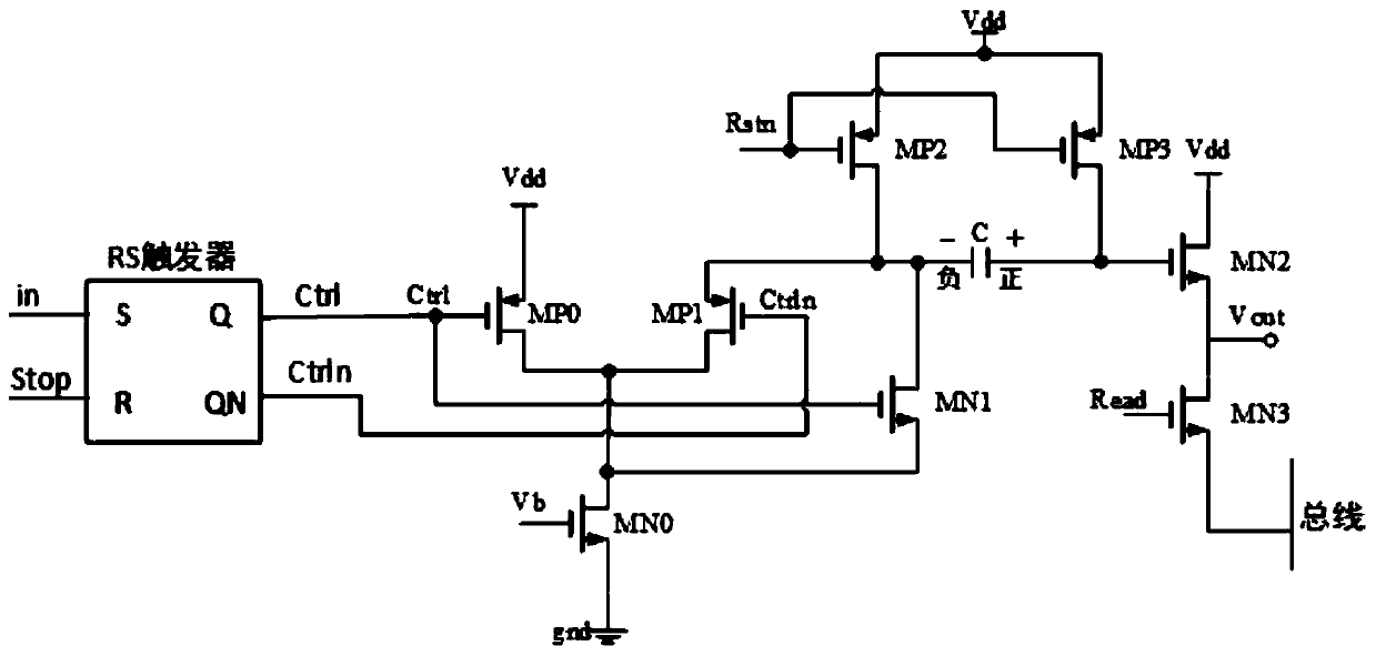
The invention discloses a compact type time to analog conversion circuit applied to a single-photon detector. The compact type time to analog conversion circuit applied to the single-photon detector comprises an RS trigger, a timing capacitor C and eight MOS transistors, wherein the MP0 and the MP1 form a differential structure as an input stage; the MN1 and the MP1 form a complementary CMOS switch; the three MOS transistors including the MP0, the MN1 and the MP1 form a control logic together, so that discharging of the timing capacitor C is controlled; the MP2 and the MP3 are used as two PMOSswitches used for controlling the reset operation of the timing capacitor C; and the MN2 and the MN3 form a source-level follower used for reading voltage on the timing capacitor C. The compact typetime to analog conversion circuit applied to the single-photon detector in the invention is small in capacitance area, small in transistor number and simple in structure; the effect of greatly reducing the area of a circuit layout is achieved; the circuit density and integrity are improved; fill factors of picture elements are effectively increased; simultaneously, the overall power consumption ofthe circuit is also reduced; the manufacture cost is low; the performance consistence of various circuits is good; and the yield is high.

Description

technical field [0001] The invention relates to a compact time-to-analog conversion circuit for measuring photon flight time based on analog timing technology, belonging to the technical field of single photon detection. Background technique [0002] Single-photon avalanche photodiode (Single-Photon Avalanche Diode, SPAD) has significant advantages such as large avalanche gain, fast response speed, high detection sensitivity, low cost, and low power consumption, and can obtain time and space information of photon signals. Aspects such as laser ranging and 3D imaging show broad application prospects. [0003] The time-of-flight measurement method based on the SPAD detector imaging technology mainly adopts the time-to-digital conversion method (Time to Digital Convert, TDC), although the TDC circuit has a high time resolution, strong ability to suppress noise and anti-interference However, due to its complex structure, a large number of tubes, increased power consumption, and...

Claims


Application Information

Patent Timeline
Patent Type & Authority Patents(China)
IPC IPC(8): G04F10/00
CPCG04F10/005
Inventor 吴仲徐跃李鼎朱思慧
Owner NANJING UNIV OF POSTS & TELECOMM
Learn More