Semi-conductor perovskite solar cell and preparing method thereof

A solar cell and perovskite technology, applied in the field of solar cells, can solve the problems of complicated process and expensive perovskite solar cell materials

Inactive Publication Date: 2014-10-08
HUAZHONG UNIV OF SCI & TECH
View PDF4 Cites 43 Cited by
  • Summary
  • Abstract
  • Description
  • Claims
  • Application Information

AI Technical Summary

Problems solved by technology

[0007] The invention provides a semiconductor perovskite solar cell and a preparation method thereof, which solves the problems of expensive materials and complex processes of the existing perovskite solar cells, and can maintain a relatively high photoelectric conversion efficiency. The photoelectric conversion efficiency of the battery is increased to more than 10%

Method used


Image

  • Semi-conductor perovskite solar cell and preparing method thereof
  • Semi-conductor perovskite solar cell and preparing method thereof
  • Semi-conductor perovskite solar cell and preparing method thereof

Examples


Embodiment 1

[0077] Embodiment 1, comprises the steps:

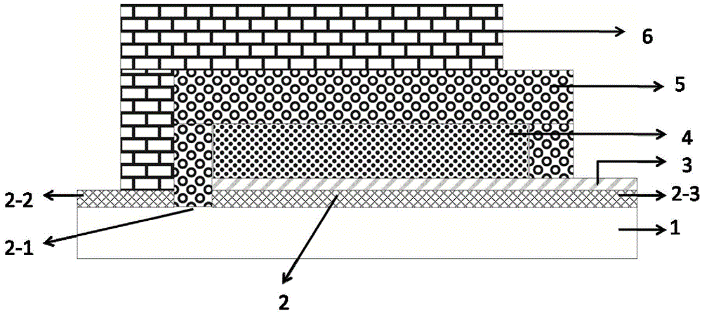
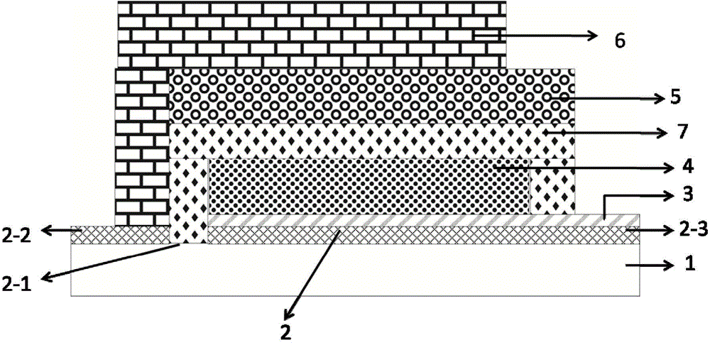
[0078] (1) Preparation of the electrode area step: on the commercially available FTO glass, grind it with a grinding wheel, etch a 2mm wide etching groove in the conductive layer, divide the conductive layer on the glass surface into a counter electrode area and a working electrode area, and then The etched FTO glass is cleaned;

[0079] (2) The step of preparing the hole blocking layer: use 0.05mol / L tetraisopropyl titanate ethanol solution as a precursor to spin-coat a layer of precursor film on the working electrode area, and sinter at 450°C for 60 minutes to form a thickness A hole blocking layer of 10nm;

[0080] (3) The step of preparing the mesoporous electron collection layer: using zinc oxide nanoparticle slurry with a particle size of 10 nm, depositing a layer of zinc oxide nanoparticle layer on the hole blocking layer by spin coating, and sintering at 400° C. for 60 minutes, Form a mesoporous electron collection layer wi...

Embodiment 2

[0088] Embodiment 2, comprises the steps:

[0089](1) Preparation of the electrode area step: on the commercially available FTO glass, use a grinding wheel to polish, etch a 2mm wide etching groove in the conductive layer, divide the conductive layer on the glass surface into a counter electrode area and a working electrode area, and then Clean the etched FTO glass;

[0090] (2) The step of preparing the hole blocking layer: using 1 mol / L tetraisopropyl titanate ethanol solution as a precursor, spin-coating a layer of precursor film on the working electrode area, and sintering at 550° C. for 10 minutes, forming a hole blocking layer with a thickness of 100 nm;

[0091] (3) The step of preparing the mesoporous electron collection layer: use a tin oxide nanoparticle slurry with a particle size of 100 nm, deposit a layer of tin oxide nanoparticle layer on the hole blocking layer by screen printing, and sinter at 550 ° C for 10 minutes , forming a mesoporous electron collection ...

Embodiment 3

[0097] Embodiment 3, comprises the steps:

[0098] (1) Preparation of the electrode area step: on the commercially available FTO glass, grind it with a grinding wheel, etch a 2mm wide etching groove in the conductive layer, divide the conductive layer on the glass surface into a counter electrode area and a working electrode area, and then The etched FTO glass is cleaned;

[0099] (2) The step of preparing the hole blocking layer: use 0.05mol / L tetraisopropyl titanate ethanol solution as a precursor to spin coat a layer of precursor film on the working electrode area, and sinter at 500°C for 30 minutes to form a thickness A hole blocking layer of 60nm;

[0100] (3) The step of preparing the mesoporous electron collection layer: use a titanium dioxide nanoparticle slurry with a particle size of 20 nm, deposit a layer of titanium dioxide nanoparticle layer on the hole blocking layer by spin coating, and sinter at 500 ° C for 30 minutes to form a thickness 400nm mesoporous elec...


PUM


Abstract

The invention provides a semi-conductor perovskite solar cell and a preparing method thereof and belongs to the field of solar cells. The semi-conductor perovskite solar cell solves the problems that materials of an existing perovskite solar cell are high in price, and the process is complex, and meanwhile keeps the high photoelectric conversion efficiency. The semi-conductor perovskite solar cell sequentially comprises a substrate, a conducting layer, a hole barrier layer, a mesoporous electron collecting layer, a mesoporous hole collecting layer and a mesoporous back electrode layer from bottom to top. The preparing method of the semi-conductor perovskite solar cell comprises the steps of preparing an electrode region, the hole barrier layer, the mesoporous electron collecting layer, the mesoporous hole collecting layer, the mesoporous back electrode layer and light-absorbing materials filled with perovskite. According to the semi-conductor perovskite solar cell, a mesoporous insulating layer is additionally arranged, and the step of preparing the mesoporous insulating layer is added to the preparing method. The semi-conductor perovskite solar cell solves the problems that the materials of the existing perovskite solar cell are high in price, and the process is complex, and open-circuit voltage, short-circuit current and fill factors of the cell are increased.

Description

technical field [0001] The invention belongs to the field of solar cells, in particular to a semiconductor perovskite solar cell and a preparation method thereof. Background technique [0002] With the rapid development of the economy, the human demand for energy is increasing day by day, and the environment-friendly renewable energy has been widely concerned, among which the photovoltaic industry is developing rapidly. A solar cell is a device that converts sunlight energy into electrical energy. When the light shines on the light-receiving surface of the solar cell, the solar cell converts the absorbed light energy into electrical energy to generate photovoltage and photocurrent, and its photoelectric conversion efficiency PCE=J SC ×V OC ×FF, where, the short-circuit current density J of the battery SC , open circuit voltage V OC , Fill factor FF. [0003] Traditional solar cells require a large amount of high-purity inorganic semiconductor materials, such as high-puri...

Claims


Application Information

Patent Timeline
Patent Type & Authority Applications(China)
IPC IPC(8): H01L51/42H01L51/44H01L51/46H01L51/48
CPCY02E10/549H10K30/00H10K30/81H10K2102/00H10K85/50
Inventor 赵志新刘宗豪张蒙
Owner HUAZHONG UNIV OF SCI & TECH
Why Eureka
Try Eureka