Processing method and circuit board of gold finger with suspended structure

A technology of suspended structure and processing method, which is applied in the direction of multi-layer circuit manufacturing, printed circuit components, electrical connection printed components, etc., can solve the problems of resource waste cost, strong limitation, poor versatility, etc. The effect of strong versatility, reducing cost and waste of resources

Active Publication Date: 2017-10-10
SHENNAN CIRCUITS
View PDF8 Cites 0 Cited by
  • Summary
  • Abstract
  • Description
  • Claims
  • Application Information

AI Technical Summary

Problems solved by technology

[0005] Embodiments of the present invention provide a processing method and a circuit board of a gold finger with a suspended structure, so as to solve the technical problems of existing gold finger circuit boards, which have strong limitations, poor versatility, and easily lead to resource waste and cost increase.

Method used


Image

  • Processing method and circuit board of gold finger with suspended structure
  • Processing method and circuit board of gold finger with suspended structure
  • Processing method and circuit board of gold finger with suspended structure

Examples


Embodiment 1

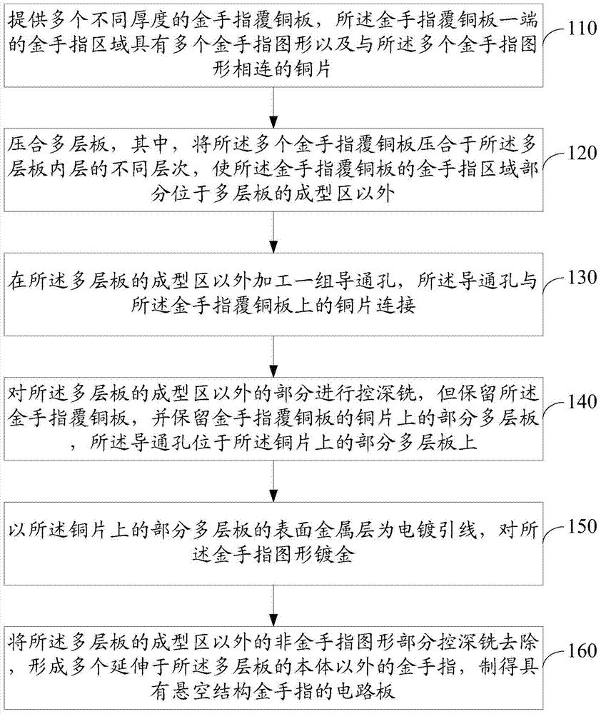
[0027] Please refer to figure 1 , an embodiment of the present invention provides a method for processing a gold finger with a suspended structure, which may include:

[0028] 110. Provide multiple gold finger copper clad laminates with different thicknesses, the gold finger area at one end of the gold finger copper clad laminate has multiple gold finger patterns and copper sheets connected to the multiple gold finger patterns.

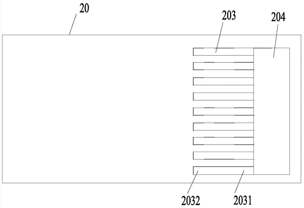
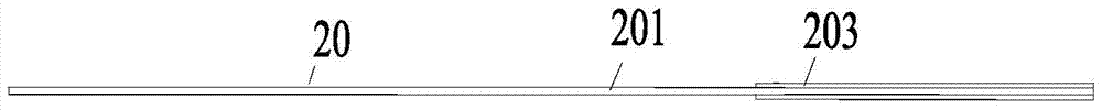
[0029] In the embodiment of the present invention, the gold finger copper clad laminate provided is as follows Figure 2a and 2b As shown, the gold finger copper clad laminate 20 includes an insulating medium 201 in the middle and metal layers on both sides, one end of which is designed with a gold finger area, and the metal layer in the gold finger area is processed into a plurality of gold finger patterns 203 and connected with a plurality of gold finger The copper sheet 204 that is pattern-connected, and the metal layer outside the gold finger ar...

Embodiment 2

[0054] Please refer to Figure 2g and 2h , an embodiment of the present invention provides a circuit board with gold fingers in a suspended structure, the circuit board may include:

[0055] The circuit board body 30 and the gold finger 37 of the suspended structure, one end of the gold finger of the suspended structure is embedded in the circuit board body, and the other end extends from one side of the circuit board body, and the gold finger of the suspended structure includes a multi-layer , each layer includes at least one gold finger 37, and the gold finger 37 is a gold-plated copper clad laminate structure.

[0056] The circuit board body may include multiple circuit layers, and each gold finger 37 may be connected to at least one of the multiple circuit layers through a metallized through hole 35 .

[0057] The circuit board provided by the embodiment of the present invention can be manufactured by the method of the first embodiment. For a more detailed description, ...


PUM


Abstract

The invention discloses a processing method and a circuit board of a gold finger with a suspended structure, in order to solve the technical problems of existing gold finger circuit boards, such as strong limitations, poor versatility, and easy resource waste and cost increase. The method includes: providing a plurality of gold-finger copper-clad laminates with different thicknesses; laminating the multi-layer board, wherein the multiple gold-finger copper-clad boards are laminated to different layers of the inner layer of the multi-layer board; A group of via holes are processed outside the forming area of ​​the board, and the via holes are connected with the copper sheet and the gold finger pattern on the gold finger copper clad board; controlled depth milling removes the part outside the forming area of ​​the multi-layer board, However, the gold finger copper clad laminate is retained; the gold finger pattern is plated with gold; each gold finger pattern extended from the gold finger copper clad laminate is processed into a gold finger by controlled deep milling, and a circuit board with a suspended structure gold finger is obtained.

Description

technical field [0001] The invention relates to the technical field of circuit boards, in particular to a method for processing golden fingers with a suspended structure and a circuit board. Background technique [0002] At present, the structural design of printed circuit board (PCB) boards with gold fingers generally adopts the method of designing the gold fingers within the forming area of ​​the surface layer of the circuit board. The gold finger that provides the plug-in function should match the size of the plug-in interface. The thickness of the gold-finger circuit board should be consistent with the opening height of the plug-in interface. When the opening height of the plug-in interface is fixed, the circuit where the gold finger is located The plate thickness is thus fixed. [0003] When the thickness of the gold finger circuit board needs to be increased to achieve multi-functional requirements, the supporting plug-in interface equipment needs to be completely cha...

Claims


Application Information

Patent Timeline
Patent Type & Authority Patents(China)
IPC IPC(8): H05K3/40H05K3/46H05K1/11
Inventor 刘宝林郭长峰丁大舟缪桦
Owner SHENNAN CIRCUITS
Why Eureka
Try Eureka