Processing method of circuit board gold finger and gold finger circuit board

A processing method and gold finger technology, applied in the direction of multi-layer circuit manufacturing, printed circuit components, electrical connection printed components, etc., can solve the problems of resource waste cost, strong limitations, poor versatility, etc., to save resources and costs, The effect of strong versatility, reducing cost and waste of resources

Active Publication Date: 2017-12-29
SHENNAN CIRCUITS
View PDF8 Cites 0 Cited by
  • Summary
  • Abstract
  • Description
  • Claims
  • Application Information

AI Technical Summary

Problems solved by technology

[0005] Embodiments of the present invention provide a method for processing a golden finger of a circuit board and a golden finger circuit board, so as to solve the problem of existing golden finger circuit boards, which have strong limitations, poor versatility, and easily lead to resource waste and cost increase. technical problem

Method used


Image

  • Processing method of circuit board gold finger and gold finger circuit board
  • Processing method of circuit board gold finger and gold finger circuit board
  • Processing method of circuit board gold finger and gold finger circuit board

Examples


Embodiment 1

[0027] Please refer to figure 1 , an embodiment of the present invention provides a method for processing a gold finger of a circuit board, which may include:

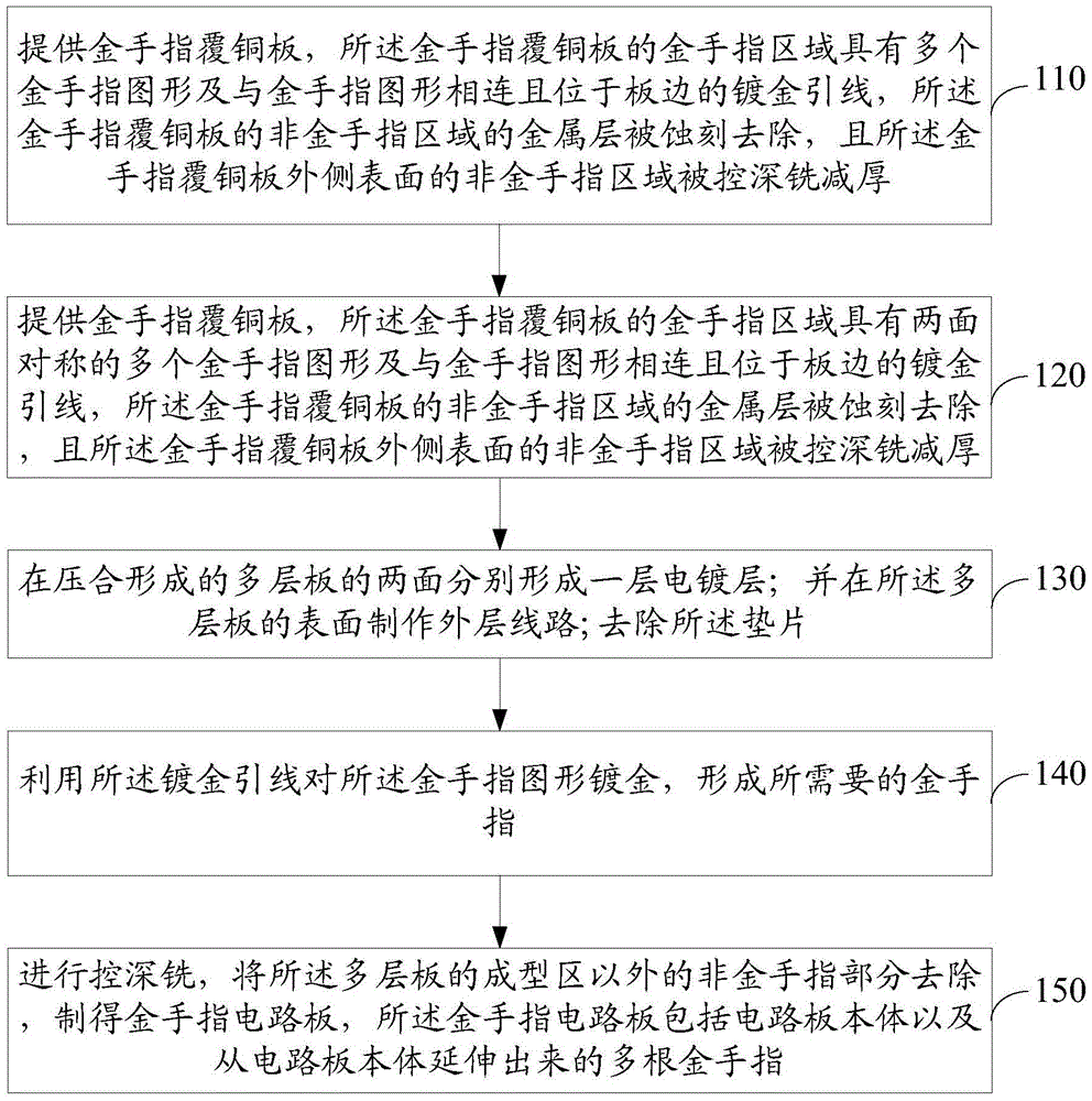
[0028] 110. Provide a gold-finger copper-clad board, the gold-finger area of ​​the gold-finger copper-clad board has a plurality of gold-finger patterns and gold-plated leads connected to the gold-finger patterns and located on the edge of the board, the non-gold-finger area of ​​the gold-finger copper-clad board The metal layer is removed by etching, and the non-gold finger area on the outer surface of the gold finger copper-clad laminate is controlled to be deep-milled to reduce the thickness.

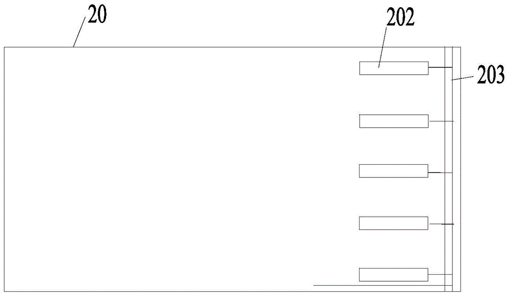
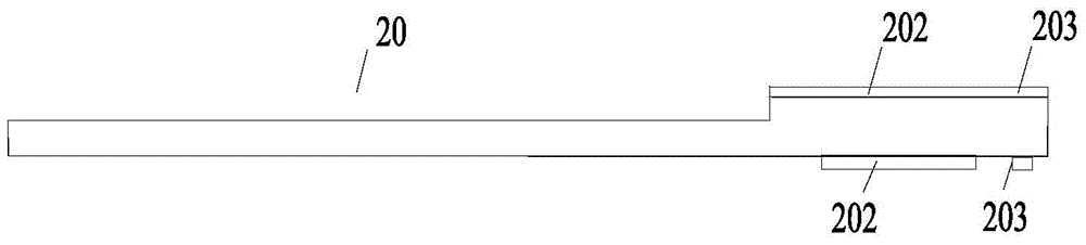
[0029] In an implementation manner of the embodiment of the present invention, such as Figure 2a and 2b As shown, according to the opening height of the plug-in interface of the device, a gold finger copper clad laminate 20 of corresponding thickness can be prepared. The gold finger copper clad laminate can specifically be...

Embodiment 2

[0053] Please refer to Figure 2g and 2h , an embodiment of the present invention provides a golden finger circuit board, which may include:

[0054] The circuit board body 30, on one side of the circuit board body, two groups of gold fingers extend from both sides of the circuit board body, each group includes at least one gold finger 37, and the gold finger 37 is a gold-plated copper clad laminate structure .

[0055] The circuit board body may include multiple circuit layers (the internal multiple circuit layers are not shown in the figure).

[0056] The golden finger 37 can be connected with the outer circuit 307 of the circuit board.

[0057] The circuit board provided by the embodiment of the present invention can be manufactured by the method of the first embodiment. For a more detailed description, please refer to Embodiment 1.

[0058] Above, the embodiment of the present invention provides a golden finger circuit board, which achieves the following technical eff...


PUM


Abstract

The invention discloses a processing method of a gold finger of a circuit board and a gold finger circuit board to solve the existing problems of the existing gold finger circuit board, which have strong limitations, poor versatility, and easily lead to resource waste and cost increase. question. The method includes: providing a gold finger copper clad laminate with a gold finger pattern and gold-plated leads, the non-gold finger area on the outer surface of which is controlled to be deep-milled and reduced in thickness; in the controlled deep-milled thickened area, the outer dielectric layer and the outer metal layer are stacked ; Laminate the inner circuit layer and the inner dielectric layer between the non-gold finger areas of the two gold finger copper clad laminates; set a gasket between the gold finger areas of the two gold finger copper clad laminates; then, press to form a multi-layer board; make the outer layer circuit; gold-plate the gold finger pattern to form a gold finger; control deep milling to remove the non-gold finger part outside the forming area of ​​the multi-layer board to obtain a gold finger circuit board, the gold finger circuit board includes the circuit board body And the extended golden fingers.

Description

technical field [0001] The invention relates to the technical field of circuit boards, in particular to a method for processing a golden finger of a circuit board and a golden finger circuit board. Background technique [0002] At present, the structural design of printed circuit board (PCB) boards with gold fingers generally adopts the method of involving the gold fingers within the forming area of ​​the surface layer of the circuit board. The gold finger that provides the plug-in function should match the size of the plug-in interface. The thickness of the gold-finger circuit board should be consistent with the opening height of the plug-in interface. When the opening height of the plug-in interface is fixed, the circuit where the gold finger is located The plate thickness is thus fixed. [0003] When the thickness of the gold finger circuit board needs to be increased to achieve multi-functional requirements, the supporting plug-in interface equipment needs to be complet...

Claims


Application Information

Patent Timeline
Patent Type & Authority Patents(China)
IPC IPC(8): H05K3/40H05K3/46H05K1/11
Inventor 刘宝林郭长峰丁大舟缪桦
Owner SHENNAN CIRCUITS
Why Eureka
Try Eureka