Gold finger processing method and gold finger circuit board

A processing method and gold finger technology, applied in the directions of printed circuit components, electrical connection printed components, and electrical connection formation of printed components, can solve the problems of waste of resources, poor versatility, strong limitations, etc., and save resources and costs. , Reduce costs and waste of resources, and have strong versatility

Active Publication Date: 2018-06-26
SHENNAN CIRCUITS
View PDF8 Cites 0 Cited by
  • Summary
  • Abstract
  • Description
  • Claims
  • Application Information

AI Technical Summary

Problems solved by technology

[0005] Embodiments of the present invention provide a gold finger processing method and a gold finger circuit board to solve the existing technical problems of the existing gold finger circuit boards, which have strong limitations, poor versatility, and easily lead to resource waste and cost increase.

Method used


Image

  • Gold finger processing method and gold finger circuit board
  • Gold finger processing method and gold finger circuit board
  • Gold finger processing method and gold finger circuit board

Examples


Embodiment 1

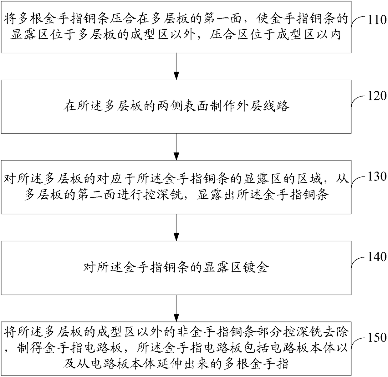
[0026] Please refer to figure 1 , the embodiment of the present invention provides a gold finger processing method, which may include:

[0027] 110. Press a plurality of gold finger copper strips on the first surface of the multilayer board, so that the exposed area of ​​the gold finger copper strips is located outside the forming area of ​​the multilayer board, and the pressing area is located inside the forming area.

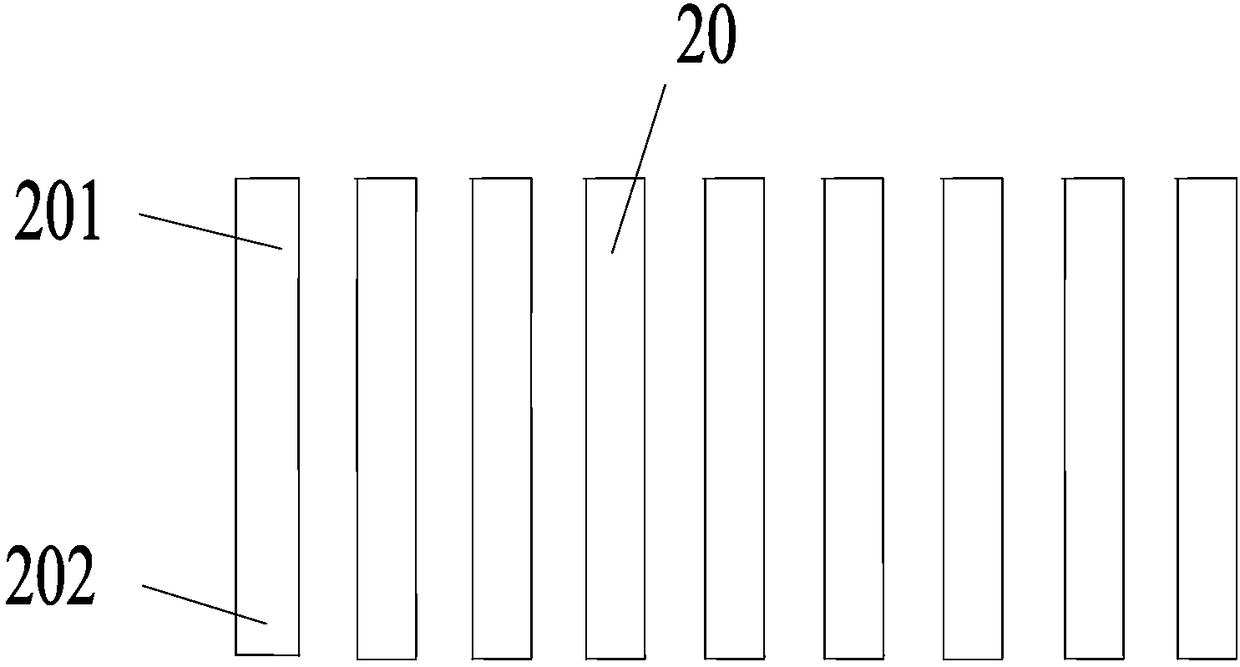
[0028] In an implementation manner of the embodiment of the present invention, such as Figure 2a As shown, copper plates of corresponding thickness can be prepared according to the opening height of the plug-in interface of the equipment; multiple gold finger copper strips 20 can be milled out from the copper plate according to the required shape of the gold fingers by using a controlled depth milling process.

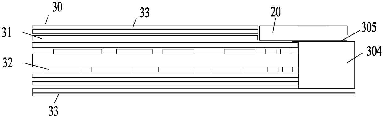
[0029] Such as Figure 2b Shown is the pressing step of the embodiment of the present invention. In the pressing step, a plurality of gold finger c...

Embodiment 2

[0051] Please refer to Figure 2f with 2g , an embodiment of the present invention provides a golden finger circuit board, which may include:

[0052] The circuit board body 30 and at least one suspended gold finger 37, one end of the suspended gold finger 37 is embedded in the circuit board body 30, and the other end extends from one side of the circuit board body 30, the suspended gold finger 37 is a gold-plated copper strip structure.

[0053] The circuit board body may include multiple circuit layers.

[0054] The suspended golden fingers 37 can be connected with the outer circuit of the circuit board body.

[0055] The circuit board provided by the embodiment of the present invention can be manufactured by the method of the first embodiment. For a more detailed description, please refer to Embodiment 1.

[0056] Above, the embodiment of the present invention provides a golden finger circuit board, which achieves the following technical effects:

[0057] The thicknes...


PUM


Abstract

The invention discloses a processing method of a gold finger, and a gold finger circuit board, for solving the technical problems of quite high restrictions, very poor versatility and high proneness to waste of resources and increase of the cost existing in a conventional gold finger circuit board. The method comprises the following steps: pressing multiple gold finger copper bars on the first surface of a multilayer board to enable the exposure areas of the gold finger copper bars to be disposed outside the formation area of the multilayer board, wherein pressing areas are disposed in the formation area; manufacturing external-layer lines on the surfaces at the two sides of the multilayer board; for the area, which is opposite to the exposure areas of the gold finger copper bars, of the multilayer board, performing controlled depth milling from the second surface of the multilayer board to expose the gold finger copper bars; gilding the exposure areas of the gold finger copper bars; and removing a non gold finger copper bar portion outside the formation area of the multilayer board so as to prepare the gold finger circuit board, wherein the gold finger circuit board comprises a circuit board body and multiple gold fingers extending from the circuit board body.

Description

technical field [0001] The invention relates to the technical field of circuit boards, in particular to a gold finger processing method and a gold finger circuit board. Background technique [0002] At present, the structural design of printed circuit board (PCB) boards with gold fingers generally adopts the method of designing the gold fingers within the forming area of ​​the surface layer of the circuit board. The gold finger that provides the plug-in function should match the size of the plug-in interface. The thickness of the gold-finger circuit board should be consistent with the opening height of the plug-in interface. When the opening height of the plug-in interface is fixed, the circuit where the gold finger is located The plate thickness is thus fixed. [0003] When the thickness of the gold finger circuit board needs to be increased to achieve multi-functional requirements, the supporting plug-in interface equipment needs to be completely changed, which is a waste...

Claims


Application Information

Patent Timeline
Patent Type & Authority Patents(China)
IPC IPC(8): H05K3/40H05K1/11
Inventor 刘宝林郭长峰丁大舟缪桦
Owner SHENNAN CIRCUITS
Why Eureka
Try Eureka