Processing method for dangling gold fingers and circuit board

A golden finger and circuit board technology, which is applied in the directions of printed circuit components, electrical connection printed components, and the formation of printed component electrical connections, can solve the problems of resource waste cost, poor versatility, strong limitations, etc., and achieve resource and cost saving , Reduce cost and waste of resources, strong versatility

Active Publication Date: 2015-10-14
SHENNAN CIRCUITS
View PDF8 Cites 3 Cited by
  • Summary
  • Abstract
  • Description
  • Claims
  • Application Information

AI Technical Summary

Problems solved by technology

[0005] Embodiments of the present invention provide a method for processing a suspended gold finger and a circuit board, so as to solve the existing technical problems of the existing gold finger circuit board, which have strong limitations, poor versatility, and easily lead to resource waste and cost increase.

Method used


Image

  • Processing method for dangling gold fingers and circuit board
  • Processing method for dangling gold fingers and circuit board
  • Processing method for dangling gold fingers and circuit board

Examples


Embodiment 1

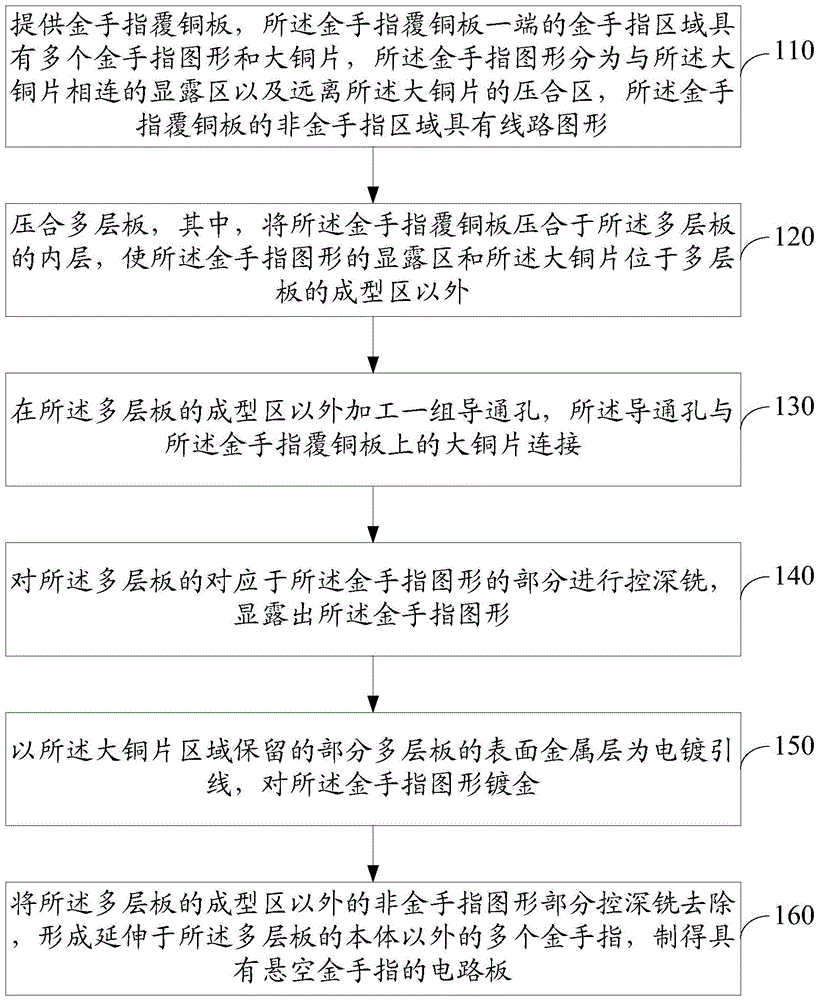
[0027] Please refer to figure 1 , The embodiment of the present invention provides a method for processing a floating gold finger, which may include:

[0028] 110. A gold finger copper clad laminate is provided. The gold finger area at one end of the gold finger copper clad laminate has a plurality of gold finger patterns and large copper pieces, and the gold finger patterns are divided into exposed areas connected to the large copper pieces and far away from all areas. In the pressing area of ​​the large copper sheet, the non-gold finger area of ​​the gold finger copper clad laminate has a circuit pattern.

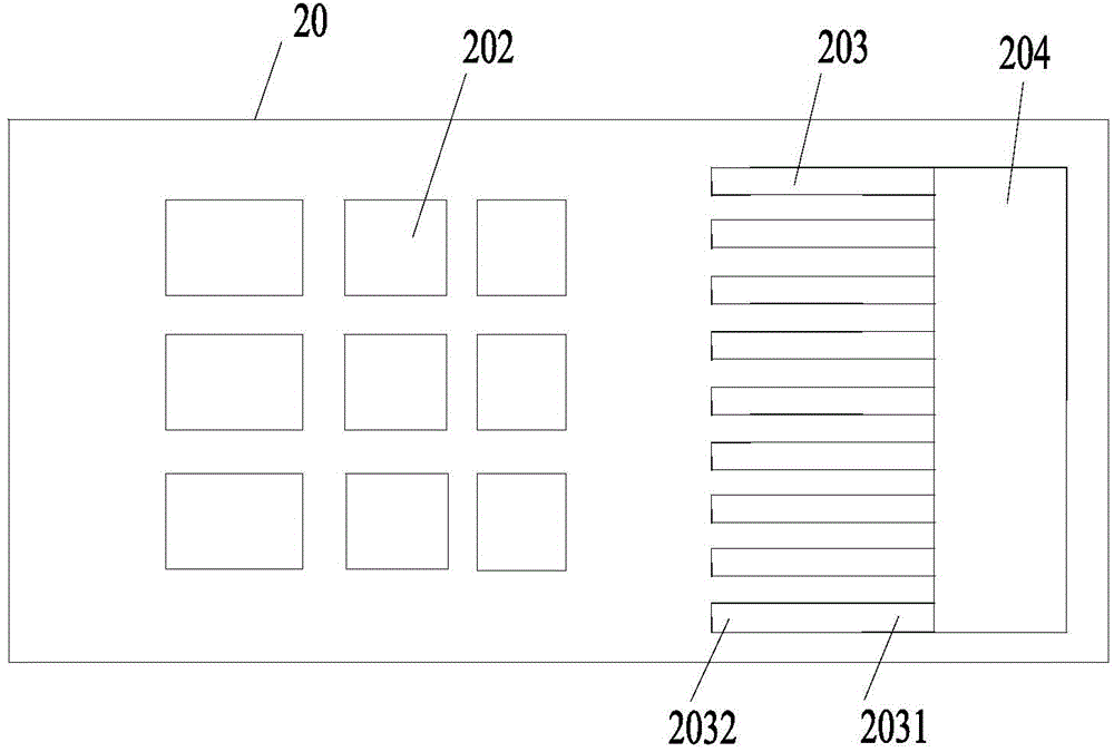
[0029] In the embodiment of the present invention, the provided gold finger copper clad laminate such as Figure 2a As shown, the gold finger copper clad laminate 20 includes an insulating medium in the middle and metal layers on both sides. One end is designed with a gold finger area. The metal layer of the gold finger area is processed into multiple gold finger patterns 203 a...

Embodiment 2

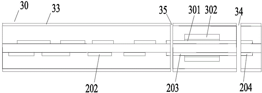
[0052] Please refer to Figure 2d with 2e , The embodiment of the present invention provides a circuit board with floating gold fingers, the circuit board may include:

[0053] The circuit board body 30 and at least one suspended gold finger 37, one end of the suspended gold finger 37 is embedded in the circuit board body 30, and the other end extends from a side wall of the circuit board body 30, the gold finger 37 is Gold-plated copper clad laminate structure.

[0054] The circuit board body may include multiple circuit layers, and each gold finger 37 can be connected to at least one of the multilayer circuit layers through a metalized through hole 35.

[0055] The circuit board provided by the embodiment of the present invention can be manufactured by the method of the first embodiment. For more detailed description, please refer to the first embodiment.

[0056] Above, the embodiment of the present invention provides a circuit board with floating gold fingers, which adopts the go...


PUM


Abstract

The present invention discloses a processing method for dangling gold fingers and a circuit board so as to solve the technical problems of existing gold finger circuit boards that limitation is strong, versatility is poor, waste of resources is likely to be incurred and the cost is increased. The method comprises: pressing a gold finger copper clad laminate with a gold finger pattern to an inner layer of a multilayer board; processing a set of via holes outside a formed region of the multilayer board, wherein the via holes are connected with the gold finger pattern by a large copper sheet on the gold finger copper clad laminate; exposing the gold finger pattern by depth control milling; plating the gold finger pattern with gold; and removing non-gold finger patterns outside the formed region of the multilayer board by the depth control milling to form the gold fingers and obtain a circuit board with the dangling gold fingers.

Description

Technical field [0001] The invention relates to the technical field of circuit boards, in particular to a method for processing suspended gold fingers and a circuit board. Background technique [0002] At present, the structure design of printed circuit board (PCB) boards with gold fingers generally adopts the method of involving the gold fingers in the surface forming area of ​​the circuit board. The gold finger that provides the plug-in function should match the size of the plug-in interface. The thickness of the gold-finger circuit board should be consistent with the opening height of the plug-in interface. When the opening height of the plug-in interface is fixed, the circuit where the gold finger is located The plate thickness is therefore fixed. [0003] When the gold finger circuit board needs to increase the board thickness to achieve multi-function requirements, the supporting plug-in interface equipment must be completely changed, which is a waste of resources and costs;...

Claims


Application Information

Patent Timeline
Patent Type & Authority Applications(China)
IPC IPC(8): H05K3/40H05K1/11
Inventor 刘宝林郭长峰丁大舟缪桦
Owner SHENNAN CIRCUITS
Why Eureka
Try Eureka