Organic electroluminescent transistor array substrate and manufacturing method thereof, and display device

A transistor array and fabrication method technology, which is applied in the fields of electric solid state device, semiconductor/solid state device manufacturing, circuit, etc., can solve the problem that carriers are not controlled by the gate layer, and achieve the effect of avoiding mutual influence

Active Publication Date: 2015-10-21
BOE TECH GRP CO LTD
View PDF3 Cites 1 Cited by
  • Summary
  • Abstract
  • Description
  • Claims
  • Application Information

AI Technical Summary

Problems solved by technology

[0004] The purpose of the present invention is to provide an organic electroluminescent transistor array substrate and its manufacturing method, and a display device to solve the problem that the carriers at the edge of the source unit in the vertical structure organic electroluminescent transistor array substrate are not controlled by the gate layer

Method used


Image

  • Organic electroluminescent transistor array substrate and manufacturing method thereof, and display device
  • Organic electroluminescent transistor array substrate and manufacturing method thereof, and display device
  • Organic electroluminescent transistor array substrate and manufacturing method thereof, and display device

Examples


Embodiment Construction

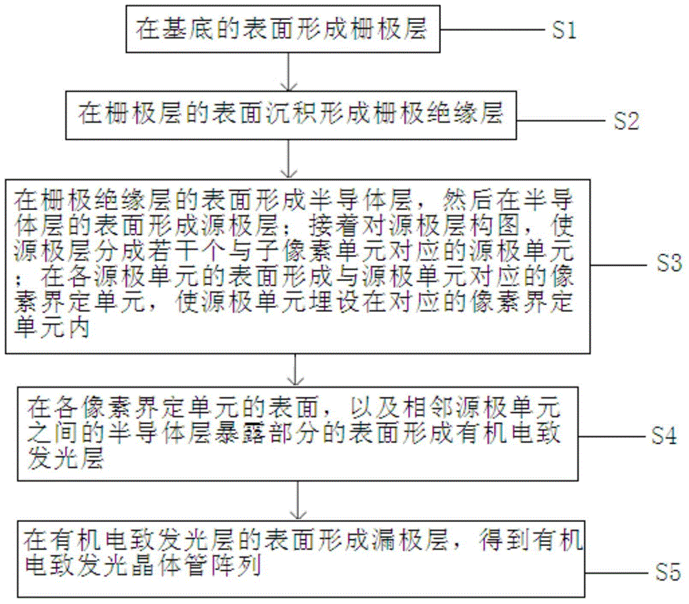
[0030] In order to further illustrate an organic electroluminescence transistor array substrate, a display device, and a manufacturing method provided by the embodiments of the present invention, a detailed description will be given below in conjunction with the accompanying drawings.

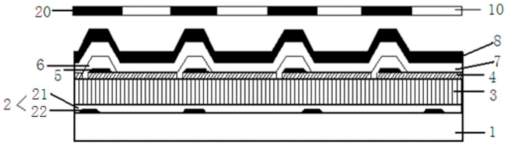
[0031] see figure 1 An organic electroluminescent transistor array substrate provided by an embodiment of the present invention includes a substrate 1, and a gate layer 2, a gate insulating layer 3, a semiconductor layer 4, a source layer, and pixels sequentially formed along the thickness direction of the substrate 1. Defining layer, organic electroluminescent layer 7 and drain layer 8, and gate layer 2 is formed on the surface of substrate 1; Wherein,

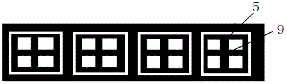
[0032] The source layer includes several source units 5 corresponding to the sub-pixel units, and the pixel defining layer includes several pixel defining units 6 corresponding to the source units 5; and each source unit 5 is embedded in the c...


PUM


Abstract

The invention discloses an organic electroluminescent transistor array substrate and a manufacturing method thereof, and a display device, and relates to the technical field of display. The organic electroluminescent transistor array substrate comprises a substrate, and a gate layer, a gate insulation layer, a semiconductor layer, a source layer, a pixel defining layer, an organic electroluminescent layer and a drain layer which are sequentially formed along the thickness direction of the substrate, wherein the gate layer is formed on the substrate. The source layer includes a plurality of source units corresponding to sub pixel units. The pixel defining layer includes a plurality of pixel defining units corresponding to the source units. Each source unit is embedded into the corresponding pixel defining unit. The organic electroluminescent layer is formed on the surfaces of the pixel defining units and the surfaces of the exposed parts of the semiconductor layer disposed between the adjacent source units.

Description

technical field [0001] The invention relates to the field of display technology, in particular to an organic electroluminescent transistor array substrate, a manufacturing method thereof, and a display device. Background technique [0002] An organic electroluminescent display is a current-type light-emitting device that uses organic electroluminescent materials as illuminants. According to the classification of driving methods, organic electroluminescent displays can be divided into passively driven organic electroluminescent displays and active driven organic electroluminescent displays; among them, the driving voltage of active driven organic electroluminescent displays is low, suitable for For high-definition and large-size display, but its manufacturing process is complicated and the production cost is high. In order to solve the problem of complex manufacturing process and high production cost of active-driven organic electroluminescent displays, researchers combined ...

Claims


Application Information

Patent Timeline
IPC IPC(8): H01L27/32H01L51/52H01L21/77H01L51/56
CPCH10K59/123H10K59/1213H10K59/122H10K59/1201H01L27/1222H01L27/1225H01L27/124H01L27/1259
Inventor 李旭远陈立强姜春生徐长成
Owner BOE TECH GRP CO LTD
Why Eureka
Try Eureka