
Grid turn-on voltage compensation circuit, display panel, driving method and display device

A gate turn-on and voltage compensation technology, applied in static indicators, instruments, etc., can solve the problems of inconsistent wiring impedance, affecting the quality of the display screen, and difference in turn-on voltage.

Active Publication Date: 2015-11-18
CHONGQING BOE OPTOELECTRONICS +1
View PDF10 Cites 21 Cited by
  • Summary
  • Abstract
  • Description
  • Claims
  • Application Information

AI Technical Summary

Problems solved by technology

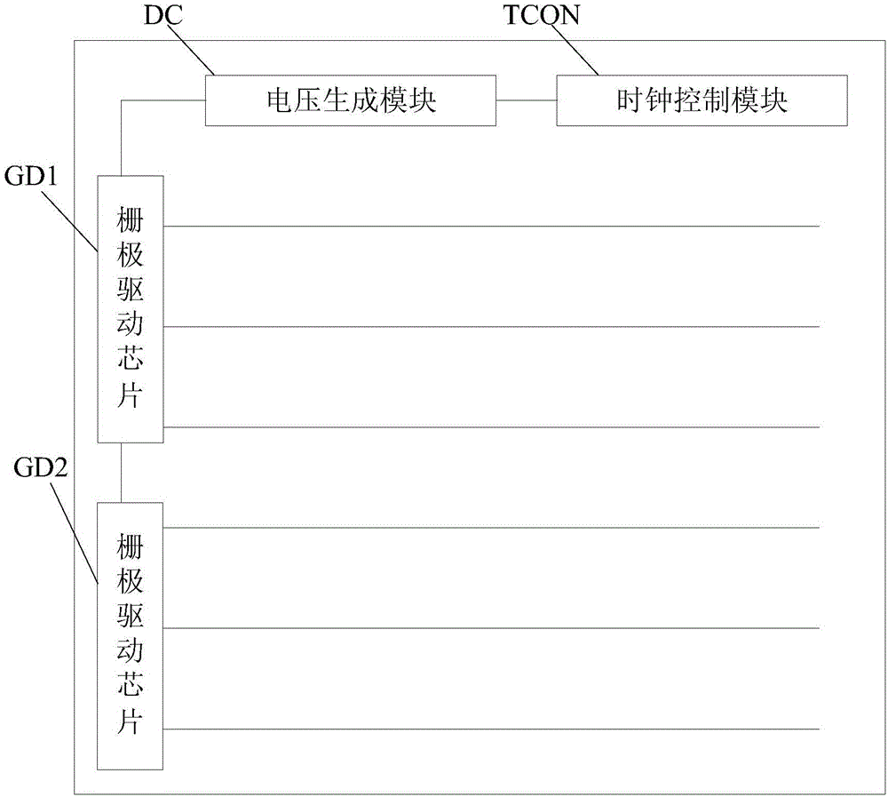
[0003] In order to realize the progressive scanning of the display panel, usually a plurality of gate drive chips are arranged in the peripheral area of ​​the display panel to input the gate turn-on voltage to the gate lines of the display area, such as figure 1 As shown, one side of the peripheral area of ​​the display panel, such as the left side, is provided with two gate drive chips GD1 and GD2, and the gate turn-on voltage is generated by the voltage generation module DC, and then output to the cascaded gate drive chips GD1 and GD2 , the gate drive chips GD1 and GD2 output gate scan signals to the gate lines of the display area in sequence under the control of the clock control module TCON to realize the progressive scan of the display panel. However, since the gate open voltage signal passes through the gate drive chip GD1 Transmission to the gate driver chip GD2. During the transfer process, due to the long wiring, the wiring impedance of the gate turn-on voltage signal on the gate driver chip GD1 is inconsistent with the trace impedance of the gate turn-on voltage signal on the gate driver chip GD2. , the gate turn-on voltage output by the gate driver chip GD1, that is, the gate scan signal, is different from the gate scan signal output by the gate driver chip GD2, so that the gate turn-on voltages output by different gate driver chips are different, resulting in The phenomenon of horizontal two-split screen affects the quality of the display screen

Method used


Image

  • Grid turn-on voltage compensation circuit, display panel, driving method and display device
  • Grid turn-on voltage compensation circuit, display panel, driving method and display device
  • Grid turn-on voltage compensation circuit, display panel, driving method and display device

Examples


Embodiment Construction

[0050] Specific implementations of the gate turn-on voltage compensation circuit, the display panel, its driving method, and the display device provided by the embodiments of the present invention will be described in detail below with reference to the accompanying drawings.

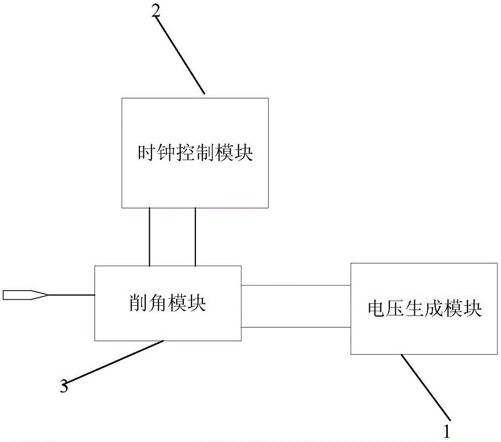
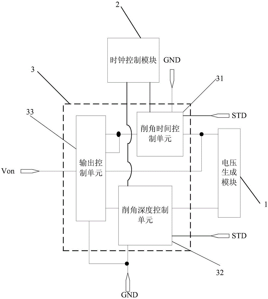
[0051] An embodiment of the present invention provides a gate turn-on voltage compensation circuit, such as figure 2 As shown, it may include: a voltage generation module 1, a clock control module 2 and a chamfering module 3; wherein,

[0052] The first voltage output end of the voltage generation module 1 is connected with the first voltage input end of the chamfering module 3, the second voltage output end of the voltage generation module 2 is connected with the second voltage input end of the chamfering module 3, and the voltage generation module 1 For correspondingly outputting the generated first voltage signal and the second voltage signal to the first voltage input terminal and the second voltage...


PUM


Abstract

The invention discloses a grid turn-on voltage compensation circuit, a display panel, a driving method of the display panel, and a display device. The grid turn-on voltage compensation circuit comprises a voltage generation module, a clock control module and a chamfering module, wherein the voltage generation module is used for outputting a generated first voltage signal to a first voltage input end of the chamfering module, and outputting a generated second voltage signal to a second voltage input end of the chamfering module; and the clock control module is used for controlling the chamfering module to output the corresponding voltage signals after chamfering at the corresponding time periods, so that chamfering depths of grid turn-on voltage signals correspondingly input to grid driving chips at different time periods are different. Since the grid turn-on voltage singles need to pass through wiring of different lengths to reach the different grid driving chips, the grid turn-on voltages, namely, grid scanning signals output to grid lines by the grid driving chips can be relatively even, thereby improving the transverse two-screen splitting phenomenon, and enhancing quality of display images.

Description

technical field [0001] The present invention relates to the field of display technology, in particular to a gate turn-on voltage compensation circuit, a display panel, a driving method thereof and a display device. Background technique [0002] At present, display technology is widely used in the display of TV, mobile phone and public information. The flat-panel display used to display the picture is vigorously promoted because of its ultra-thin and energy-saving advantages, and gate driver chips are required in most flat-panel displays. To output the gate scanning signal to control the display panel to realize the functions of progressive scanning and frame-by-frame refresh, so that the image data input to the display panel can be refreshed in real time, thereby realizing dynamic display. [0003] In order to realize the progressive scanning of the display panel, usually a plurality of gate drive chips are arranged in the peripheral area of ​​the display panel to input the ...

Claims


Application Information

Patent Timeline
Patent Type & Authority Applications(China)
IPC IPC(8): G09G3/20
CPCG09G3/2007G09G3/3225G09G3/3648G09G3/3696G09G2300/0426G09G2310/0267G09G2310/066G09G2310/067G09G2330/028
Inventor 陆旭许益祯尚飞邱海军肖利军侯帅
Owner CHONGQING BOE OPTOELECTRONICS
Learn More