Display panel and manufacturing method thereof and display device and control method thereof

A technology for display panels and display units, which can be used in identification devices, semiconductor/solid-state device manufacturing, static indicators, etc., and can solve the problems of inability to form reflections, reducing light extraction efficiency, and increasing layer structures.

Active Publication Date: 2015-11-18
BOE TECH GRP CO LTD
4 Cites 18 Cited by

AI-Extracted Technical Summary

Problems solved by technology

With this structure, the introduction of the sensor device 2 will result in more layer structures, and more masking processes must be used during manufacture; at the same time, si...

Method used

In summary, the present invention proposes a display panel and a manufacturing method thereof, a display device and a control method thereof, which can synchronously form a sensor device when the display device is formed, without additional process; especially the present invention provides a Taking advantage of the bendable characteristics of the flexible substrate, the sensor device is formed on it synchronously and attached to the top cover that can cover the light-emitting area. When the top cover is closed, the brightness data is obtained, and the compensation value is obtained and stored through calculation. Compensate according to the compensation value at the next startup, without additional process, no additional cost, and no increase in power consumption. It also protects the flexible screen while compensating for brightness.
[0074] In addition, it should be noted that the above-mentioned display unit 101 only includes the organic light-emitting diode D1, the driving transistor T1 and the switching transistor T2, and is not limited to this in fact. Often, the display unit 101 also includes a device for eliminating threshold voltage drift, Compensation circuits for problems such as inconsistency, but since these compensation circuits are usually composed of thin film transistors, their preparation can be formed synchronously with the driving transistor T1 and the switching transistor T2, so this embodiment will not repeat them here. In addition, in this embodiment, the sensing unit 201 and the display unit 101 are controlled by the same gate line, the mask used for preparing the gate metal layer requires less modification, and the arrangement of circuit components and signal lines is easier during design. But in fact, as shown in FIG. 5, the sensing unit 201 can be controlled by controlling the next line of the grid line of the display unit 101, that is, the display unit 101 is controlled by the nth (n is a natural number) grid line, and the sensing unit 201 uses The n+1th gate line is controlled, so that the nth gate line is turned on, and the display unit 101 of the nth row starts to load the display signal, and then the nth gate line is turned off, the n+1th gate line is tu...

Abstract

The embodiment of the invention discloses a display panel and a manufacturing method thereof and a flexible display device and a control method thereof. The mask film process can be reduced so that production efficiency can be enhanced and cost can be reduced. The display panel comprises display units, and sensing units which are used for detecting brightness of the display units. The sensing units and the display units are synchronously formed in different areas of the same underlying substrate.

Application Domain

Static indicating devicesSolid-state devices +3

Technology Topic

EngineeringFlexible display +1

Image

  • Display panel and manufacturing method thereof and display device and control method thereof
  • Display panel and manufacturing method thereof and display device and control method thereof
  • Display panel and manufacturing method thereof and display device and control method thereof

Examples

  • Experimental program(3)

Example Embodiment

[0062] Example one
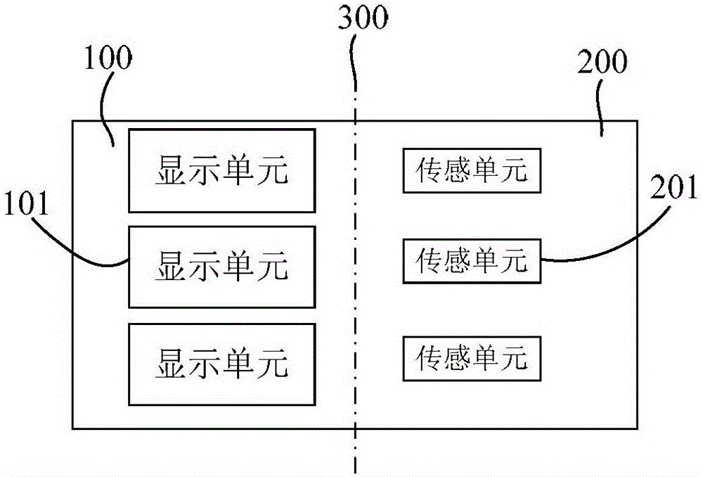
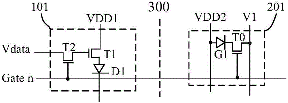
[0063] An embodiment of the present invention provides a display panel including: a display unit and a sensing unit for detecting the brightness of the display unit, and the sensing unit and the display unit are synchronously formed in different areas of the same base substrate.
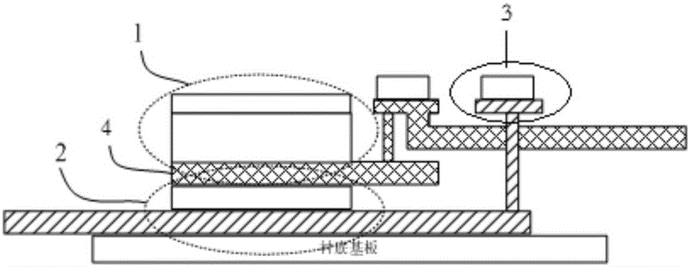
[0064] The display panel provided by the embodiment of the present invention includes a plurality of display units, and also includes sensing units synchronously formed in different areas of the same base substrate. The sensing units are used to detect the brightness of certain display units to achieve brightness detection and Compensation function. Generally speaking, the display unit mainly includes a display device and a thin film transistor that controls the operation of the display device, and a signal line. The main component of the sensing unit is a photosensitive device. The electrode of the photosensitive device and the signal line connected to the electrode can be connected to the thin film transistor. The metal layer is formed simultaneously. The photosensitive material layer of the photosensitive device is generally a semiconductor material with photosensitive characteristics, such as organic photoconductor, silicon, cadmium sulfide, zinc oxide, cadmium sulfide, etc., by selecting the active layer of the thin film transistor in the display unit It is the same material as the photosensitive material layer and can be made simultaneously through the same process. Therefore, the display panel provided by this embodiment does not need to add additional manufacturing processes due to the introduction of the sensor unit, and the sensor unit formed in synchronization with the display unit is attached to the display area by bending (or installing after cutting) at a later stage. On the top cover, after closing the top cover, the sensor unit covers the display area, and then plays the test screen to obtain the brightness data, and then plays the test screen to obtain the brightness data. The compensation value is calculated and stored. After the top cover is opened, press Set Set compensation value to compensate, so as to solve the problem of uneven brightness. How to specifically calculate the compensation value based on the brightness data, how to specifically perform the compensation, etc., can be any implementation known to those skilled in the art, which is not limited in this embodiment.
[0065] Preferably, the photosensitive material layer of the photosensitive device and the active layer of the thin film transistor in the sensing unit are selected from one of monocrystalline silicon, polycrystalline silicon or amorphous silicon, and the production is completed simultaneously.
[0066] Such as figure 2 As shown, as a preferred implementation of this embodiment, the above-mentioned base substrate is a flexible substrate, and is divided into a display area 100 and a sensing area 200 adjacent to the display area 100 by a bending line 300, and the display unit 101 Located in the display area 100, the sensing unit 201 is located in the sensing area 200. The sensing unit 201 and the display unit 101 are symmetrical about the bending line 300. Later, by bending along the bending line 300, the sensing unit 201 can cover the On the display unit 101, it is convenient to complete the brightness detection function. In addition, since the base substrate is a flexible substrate, it only needs to be bent along the bending line 300 in the later stage without cutting. Therefore, the sensing unit 201 can directly extend the signal line of the display unit 101 to the sensing area for driving. The driving circuit is additionally designed, and the signal line of the sensing unit 201 can be formed synchronously with the signal line of the display unit 101 during manufacture, and no additional process is required. Various signal lines required by the sensing unit 201 can be extended to the binding area, and connected to an external signal generating unit and a brightness data processing unit through a soft board (ie, FPC).
[0067] It should be noted that the above-mentioned base substrate is a flexible substrate, and any existing flexibilization process can be used in specific production, which is not limited in this embodiment. For example, the flexible substrate can be attached to the rigid substrate for production, and after the production process is completed, the rigid substrate can be removed from the backside.
[0068] In order for those skilled in the art to better understand the structure of the display panel provided by the embodiments of the present invention, the display panel provided by the present invention and the manufacturing method thereof will be described in detail below through specific embodiments.
[0069] Taking an OLED flexible display device as an example, the base substrate of the above-mentioned display panel is a flexible substrate, such as a PI substrate (polyimide substrate), which is divided into left and right sides along the bending line 300. One side forms the display unit 101, and the other side The sensing unit 201 is formed. The display unit 101 includes an organic light emitting diode and a first thin film transistor. The organic light emitting diode is disposed above the first thin film transistor. The first thin film transistor is a general term for thin film transistors used to form a driving circuit. The sensing unit 201 includes a photosensitive diode. And a second thin film transistor that controls the signal output of the photodiode. Wherein, the first electrode of the photodiode and the source and drain metal layer or the gate metal layer of the first thin film transistor are arranged in the same layer (if the first thin film transistor is a bottom-gate TFT, the first electrode of the photodiode and the gate metal layer are in the same layer ; If the first thin film transistor is a top-gate TFT, the first electrode of the photosensitive diode and the source and drain metal layer are in the same layer), the photosensitive layer of the photosensitive diode and the active layer of the first thin film transistor are arranged in the same layer, the photosensitive The second electrode of the diode is arranged in the same layer as the upper electrode of the organic light emitting diode away from the base substrate, wherein the first electrode of the photosensitive diode is the upper electrode, and the second electrode of the photosensitive diode is the lower electrode; the second thin film transistor mentioned above It is formed synchronously with the first thin film transistor, and there is no need to add additional manufacturing processes due to the introduction of the sensing unit. The sensing area is attached to the top cover of the display area after being bent later. After the top cover is closed, the sensing unit covers the display area, and then the test screen is played to obtain the brightness data, and the compensation value is calculated and stored in the top cover. After the cover is opened, it is compensated according to the set compensation value to solve the problem of uneven brightness.
[0070] Specific as image 3 As shown, the display unit 101 includes a driving tube T1, a switching tube T2, and an organic light emitting diode D1. A gate line (such as Gaten) is connected to the gate of the switching tube T2, and the data line Vdata is connected to the source of the switching tube T2. The drain of the driving tube T1 is connected to the gate of the driving tube T1, the source of the driving tube T1 is connected to the first working voltage VDD1, and the drain of the driving tube T1 is connected to the organic light emitting diode D1. The sensing unit 201 includes a photosensitive diode G1 and a second switch tube T0 that controls the signal output of the photosensitive diode G1. One end of the photosensitive diode G1 is connected to the second working voltage VDD2, and the other end is connected to the source of the second switch tube T0. The drain of T0 is connected to the sensing signal output line V1, and the gate of the second switching tube T0 is connected to the same gate line (such as Gaten) with the display unit 101, that is, the display unit 101 and the sensing unit 201 for testing the brightness of the display unit 101 adopt Controlled by the same gate line, the organic light-emitting diode D1 in the display unit 101 emits light while the second switch tube T0 is turned on, and the sensing unit 201 collects and outputs a brightness signal.
[0071] The driving tube T1 and the switching tube T2 (the first thin film transistor mentioned above is the collective name of the driving tube T1 and the switching tube T2), and the second switching tube T0 (that is, the second thin film transistor mentioned above) has the same structure, It is formed simultaneously during production; therefore, the cross-sectional structure of the display panel shown in Figure 4(a) only represents a first thin film transistor (the switch tube T2 is shown in the figure) and the organic light-emitting diode D1 in the display area. The second switch tube T0 and the photosensitive diode G1 are shown. The base substrate 10 is sequentially provided with a gate metal layer 11, a gate insulating layer 12, an active layer, a source and drain metal layer 14, an organic light-emitting material layer 16, and a transparent conductive layer from bottom to top. The gate metal layer 11 forms a display The gate 111 and gate line of the first thin film transistor in the area, the gate 112 of the second switch tube T0 in the sensing area, the lower electrode (first electrode 113) of the photosensitive diode G1 and the gate line extending to the sensing area; gate insulation Layer 12 forms the gate insulating layer of the first thin film transistor and the second switch tube T0 and the insulating film layer reserved in other places where insulation is needed; the active layer forms the active layer 131 of the first thin film transistor and the second switch tube T0 The active layer 132 and the photosensitive material layer 133 of the photosensitive diode G1; the source and drain metal layer 14 forms the source, drain and data lines of the first thin film transistor in the display area, the lower electrode 141 of the organic light emitting diode D1 and the first working voltage The signal line VDD1 forms the source and drain of the second switch tube T0 in the sensing area, the sensing signal output line V1 and the second working voltage signal line VDD2, the source and drain metal layer 14 is made of a reflective metal material , Can improve the light extraction efficiency; the organic light emitting material layer 16 forms the light emitting layer of the organic light emitting diode D1; the transparent conductive layer forms the upper electrode 171 of the organic light emitting diode D1 and the second electrode 172 (upper electrode) of the photosensitive diode G1.
[0072] The cross-sectional structure of another display panel provided by this embodiment is shown in FIG. 4(b). The difference is that the drain of the second switch tube T0 is connected to the first electrode 113 of the photodiode G1 through a via hole. Lower electrode).
[0073] It should be noted that FIGS. 4(a) and 4(b) simply show the up-down relationship of the film layers of the cross-section of the display panel, and do not involve details such as the pattern of a film layer. That is, what is shown in the figure is not used to limit the specific pattern of each film layer, and those skilled in the art can design according to actual conditions.
[0074] In addition, it should be noted that the above-mentioned display unit 101 only includes the organic light emitting diode D1, the driving tube T1, and the switching tube T2. In fact, it is not limited to this. Often, the display unit 101 also includes functions to eliminate threshold voltage drift and inconsistency. However, since these compensation circuits are usually also composed of thin film transistors, their preparation can be formed synchronously with the driving tube T1 and the switching tube T2, so this embodiment will not be repeated here. In addition, in this embodiment, the sensing unit 201 and the display unit 101 share the same gate line control, the mask used when preparing the gate metal layer requires less modification, and the circuit components and signal lines are easier to arrange during design. But in fact, it can also be like Figure 5 As shown, the sensor unit 201 is controlled by the next row of the gate line of the control display unit 101, that is, the display unit 101 is controlled by the nth (n is a natural number) gate line, and the sensor unit 201 is controlled by the n+1th gate line. In this way, the nth gate line is opened, the display unit 101 in the nth row starts to load display signals, and then the nth gate line is closed and the n+1th gate line is opened, and the display units 101 in the n+1th row start to load display signals. The row display unit 101 keeps emitting light, and the sensor unit controlled by the n+1th grid line located above the nth row display unit 101 collects the brightness signal, the signal is more stable, the unstable stage of the display signal loading is eliminated, and the measurement is more accurate. Similarly, the sensor unit 201 corresponding to the display unit 101 in the nth row can also be controlled by other adjacent gate lines below, such as the n+2th, n+3th, and so on.
[0075] In addition, if the drive tube T1 and the switch tube T2 are of top-gate structure, the second electrode of the photosensitive diode G1 can also be arranged in the same layer as the source and drain metal of the thin film transistor, and the photosensitive layer of the photosensitive diode G1 is still the same as the active layer of the thin film transistor. The arrangement of the same layer, the upper electrode requires the use of transparent conductive material, and it is not limited to the arrangement of the upper electrode of the organic light emitting diode D1 in the same layer.
[0076] After the above-mentioned display panel production process is completed, attach a protective film to the display panel and complete other necessary steps, bend each display panel along the bending line 300, and attach the sensing area from the back (the upper surface after bending) On the side of the top cover close to the display panel. When the top cover is opened, the sensing area of ​​the display panel is flattened and is in the same plane as the display area; when the top cover is closed, the sensing area is bent along the bending line 300 to the top of the display area, and the sensing area in the sensing area The unit 201 covers the corresponding display unit 101. At this time, the light-receiving surface of the diode G1 covers the light-emitting surface side of the organic light-emitting diode D1, and the light-emitting brightness of the organic light-emitting diode D1 is collected.
[0077] Preferably, the aforementioned sensing area 100 is located on one side of the display area 200 and is as large as the display area, for example, figure 2 As shown, the sensing area 100 is located on the right side of the display area 200, and the display area 200 is provided with a plurality of sensing units at equal intervals.
[0078] Figure 7 An alternative embodiment is shown, the sensing area 100 is located on the right side of the display area 200, the display area includes a plurality of display areas 102, and the sensing area 200 is provided with a sensing area 202 corresponding to the display area 102 one-to-one. At least one sensing unit 201 is provided in each sensing zone 202. Figure 7 The middle display area is divided into 9 display zones 102, and the sensing area 200 is correspondingly divided into 9 sensing zones 202. Each sensing zone 202 is provided with a sensing unit 201 to sense the brightness of the 9 display zones of the corresponding screen. After receiving the signal, perform steps such as amplification and analog-to-digital conversion, and finally average the value to determine the current that needs to be compensated for each partition, and perform compensation after the top cover is opened next time. The above-mentioned sensing zone 202 is not limited to being divided into 9 and can be subdivided infinitely; the sensing unit 201 provided in each sensing zone 202 is not limited to one, and multiple ones can be set, but as the subdivision of the display zone, transmission As the number of sensing units 201 increases, the computational complexity will increase accordingly.
[0079] Figure 8 with Picture 9 Another alternative embodiment is shown. The difference from the previous embodiment is that the sensing area 100 is located on both sides of the short side of the display area 200. After the top cover is closed, the area of ​​the sensing area 100 only covers Part of the area on the left and right sides of the display area 200; Picture 10 with Picture 11 A similar embodiment is also shown. The only difference is that the sensing area 100 is also located on both sides of the long side of the display area 200, that is, the display units 201 are arranged along the length direction, and the top cover on the left and the sensing The area is the same size, and the top cover on the right is larger than the size of the sensing area on the right. These two implementations can achieve the purpose of saving costs. There is no need to waste too much PI substrates in the production of the sensing part. Since the sensing units are all over or the longest distance or the shortest distance, the average value can be calculated by area. Generally perceive the brightness change trend of the screen along the horizontal or vertical direction, and compensate accordingly.
[0080] The embodiment of the present invention provides a display panel that can introduce a brightness sensor device without adding additional processes. Later, the brightness sensor device is installed on the inner side of the panel top cover by bending (or cutting and installing), and the top cover is closed Then, the sensor device is covered on the display area, and then the test screen is played to obtain the brightness data, and the compensation value is obtained through calculation and stored. After the top cover is opened, the set compensation value is compensated to solve the problem of uneven brightness. Since the sensor device receives the light emitted from one side of the display surface, the lower electrode of the light-emitting device close to the base substrate may use a reflective material to improve the light extraction efficiency.
[0081] An embodiment of the present invention also provides a display device, including any one of the above-mentioned display panels. Since the display device does not add additional processes due to the introduction of the brightness sensor device, the added value of the product can be increased on the basis of almost unchanged cost, so that the display device has a brightness adjustment and compensation function, the display brightness is more uniform, and the effect is better. The display device may be any product or component with display function, such as liquid crystal panel, electronic paper, OLED panel, mobile phone, tablet computer, television, monitor, notebook computer, digital photo frame, navigator, etc.
[0082] Further, the display device provided by the embodiment of the present invention is further provided with a brightness compensation switch, and the brightness compensation switch is used to turn on the brightness detection and compensation function. Such as Figure 8-11 As shown, the brightness compensation switch 21 can be arranged at a corner of the edge of the top cover (or panel) or other positions. The brightness compensation switch 21 may be a physical switch or a virtual switch. If it is a virtual switch, it will only be displayed on the panel without occupying physical space.
[0083] In addition, preferably, the brightness compensation switch can be optionally associated with the top cover, and when the top cover is closed, the brightness compensation switch is turned on, and the relevant program is executed in the background to realize the brightness detection and compensation function.
[0084] Alternatively, the brightness compensation switch can also be associated with the shutdown button (either physical or virtual). When receiving the user's shutdown instruction, the user will habitually close the top cover at this time, trigger the brightness compensation switch to turn on, and the display unit displays the compensation screen , The sensing unit collects the brightness signal, obtains the compensation value through calculation and stores it, and compensates according to the set compensation value after the next startup, thereby solving the problem of uneven brightness.

Example Embodiment

[0085] Example two
[0086] This embodiment provides a method for manufacturing a display panel, including: providing a base substrate; forming a display unit in a display area of ​​the base substrate, and in a sensing area adjacent to the display area on the same substrate Synchronously form the sensing unit.
[0087] Therefore, in the display panel provided by this embodiment, the sensor unit for detecting the brightness of the display unit is formed synchronously with the display unit, and there is no need to add additional manufacturing processes due to the introduction of the sensor unit. The sensor unit is bent ( Or attach it to the top cover of the display area by cutting it and install it. After closing the top cover, the sensor unit covers the display area, and then play the test screen to obtain the brightness data, and then play the test screen to obtain the brightness data, which is obtained by calculation The compensation value is stored and compensated according to the set compensation value after the top cover is opened to solve the problem of uneven brightness.
[0088] Specifically, taking a flexible display device as an example, the base substrate is a flexible substrate, the display area and the sensing area are separated by a bending line, and the sensing unit and the display unit are symmetrical about the bending line. It should be noted that the symmetry here means that a certain sensor unit and the display unit detected by the sensor unit are symmetric about the bending line during design.
[0089] The display unit includes an organic light-emitting diode and a first thin film transistor, and the sensor unit includes a photosensitive diode; the main manufacturing process of the display panel includes: a process of forming a first thin film transistor and a process of forming a light emitting diode; wherein, forming in the display area When the source and drain metal layers or gate metal layers of the first thin film transistor are formed, the first electrode of the photodiode is synchronously formed in the sensing area; when the active layer of the first thin film transistor is formed in the display area, the photodiode is synchronously formed in the sensing area The photosensitive layer; when the organic light emitting diode is formed in the display area away from the upper electrode of the base substrate, the second electrode of the photosensitive diode is synchronously formed in the sensing area. The sensor unit further includes a second thin film transistor, and the second thin film transistor is simultaneously formed in the step of forming the first thin film transistor. The specific process can refer to the description in the first embodiment, which will not be repeated here.
[0090] After the display panel manufacturing process is completed, attach a protective film to the display panel and complete other necessary steps. Bend each display panel along the bending line 300, so that the sensing area is attached from the back (the upper surface after bending) On the side of the top cover close to the display panel. When the top cover is closed, the sensing area of ​​the display panel is transformed from the flat state to overlying the display area. At this time, the brightness test screen is played, and the sensing unit collects the brightness information of the corresponding display unit, and calculates the compensation value accordingly. After the top cover is opened, it is compensated according to the set compensation value to solve the problem of uneven brightness.
[0091] The embodiment of the present invention provides a method for manufacturing a display panel, which can introduce a brightness sensor device without adding additional processes to solve the problem of uneven brightness.

Example Embodiment

[0092] Example three
[0093] The embodiment of the present invention also provides a control method of a display device. The display device includes any one of the display panels in the embodiments. That is, the display panel is also provided with a sensing unit formed in synchronization with the display unit. It is attached to the top cover of the display area by bending (or installing after cutting). The display device control method provided in this embodiment specifically includes:
[0094] Step 1. Trigger the brightness compensation switch to turn on the brightness detection compensation function; optionally, this step can trigger the brightness compensation switch by closing the top cover.
[0095] Step 2: The display panel displays a test image; optionally, the test image includes: all-white and all-black images of each primary color, but it is not limited to this, and may also be other test images for testing brightness.
[0096] Step 3: Collect and output the brightness signal through the sensing unit;
[0097] Step 4: Amplify the brightness signal and convert it into a digital signal;
[0098] Step 5. Perform average calculation of the digital signal according to the display area;
[0099] Step 6. Compensation is provided in different areas according to the calculation results.
[0100] Such as Picture 12 As shown, this embodiment illustrates the above control method through specific embodiments: S101, the user stops using the display device, S102, closes the top cover with the sensing unit, the top cover is closed to trigger the brightness compensation switch to turn on, the background brightness compensation function Turn on; S103, the display unit sequentially plays the test images, the test images generally include all black and all white images of each primary color, and may also include one or more grayscale images of the primary color; S104, the sensor unit Perform brightness detection on each test screen; S105, then turn off the sensing unit; S106, the brightness signal detected by the sensing unit is amplified by an amplifier; S107, then convert it into a digital signal through the analog-to-digital conversion module; S108, the The digital signal is sent to the chip for calculation. The calculation performed in the chip is mainly to calculate the average value by area, and calculate the compensation value according to the preset formula according to the calculation result and store it in the memory (usually flash memory); S109. When the user turns on the device next time, it is targeted at different areas Compensate according to the set compensation value.
[0101] The embodiment of the present invention preferably embeds the brightness detection function into the shutdown program, and sets the shutdown screen as the test screen required for brightness detection. When the user stops using the display device, closes the top cover with the sensor unit to trigger the brightness compensation switch Turn on, the background brightness detection and compensation function is turned on, the compensation value is calculated and stored, and the compensated screen is displayed when the user turns on the device next time. The control method provided in this embodiment conforms to the user's usage habits, and there is no need to increase the cumbersome operation and Can improve the display effect.
[0102] In summary, the present invention provides a display panel and a manufacturing method thereof, a display device and a control method thereof, which can simultaneously form a sensor device when the display device is formed without additional processes; in particular, the present invention provides a flexible substrate The characteristic of bending, the sensor device is synchronously formed on it and attached to the top cover that can cover the light-emitting area, the brightness data is obtained when the top cover is closed and the compensation value is calculated and stored, and the next time the power is turned on It is compensated according to the compensation value at any time, no additional process, no additional cost, no power consumption increase, and it plays a role in protecting the flexible screen while compensating for the brightness.

PUM

no PUM

Description & Claims & Application Information

We can also present the details of the Description, Claims and Application information to help users get a comprehensive understanding of the technical details of the patent, such as background art, summary of invention, brief description of drawings, description of embodiments, and other original content. On the other hand, users can also determine the specific scope of protection of the technology through the list of claims; as well as understand the changes in the life cycle of the technology with the presentation of the patent timeline. Login to view more.
Why Eureka
Try Eureka