Display panel, driving method thereof and display device with the display panel

A display panel and driving method technology, applied in the direction of static indicators, instruments, etc., can solve the problems of not being able to reduce the pixel area at the same time and uneven brightness of the display screen, so as to eliminate uneven luminous brightness, realize high-resolution display, and reduce walking. line effect

Active Publication Date: 2015-11-25
BOE TECH GRP CO LTD +1
View PDF4 Cites 42 Cited by
  • Summary
  • Abstract
  • Description
  • Claims
  • Application Information

AI Technical Summary

Problems solved by technology

[0004] The main purpose of the present invention is to provide a display panel and its driving method and display device to solve the problem in the prior art that the pixel area cannot be simultaneously reduced while overcoming the uneven brightness of the display screen

Method used


Image

  • Display panel, driving method thereof and display device with the display panel
  • Display panel, driving method thereof and display device with the display panel
  • Display panel, driving method thereof and display device with the display panel

Examples


Embodiment Construction

[0037] The technical solutions in the embodiments of the present invention will be clearly and completely described below in conjunction with the accompanying drawings in the embodiments of the present invention. Obviously, the described embodiments are only a part of the embodiments of the present invention, rather than all the embodiments. Based on the embodiments of the present invention, all other embodiments obtained by those of ordinary skill in the art without creative work shall fall within the protection scope of the present invention.

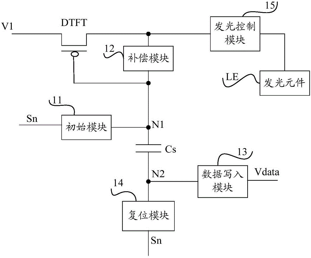
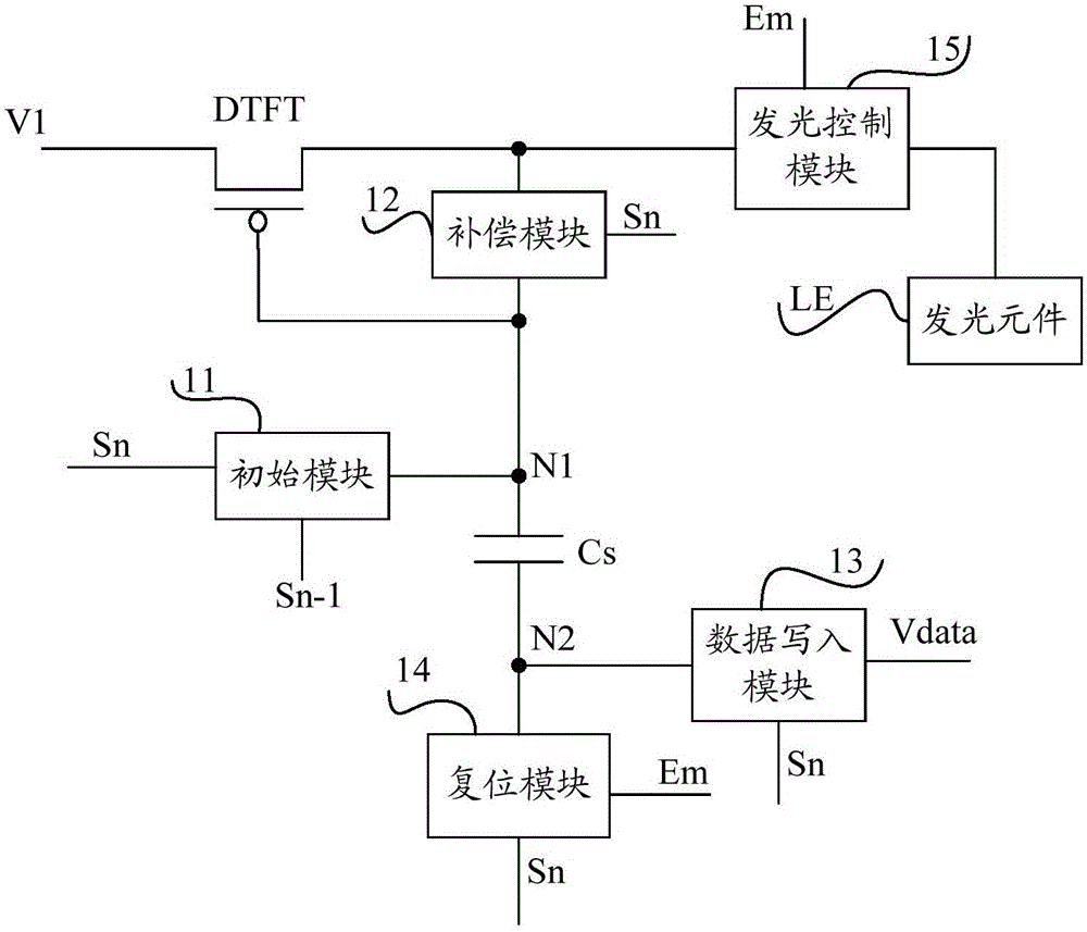
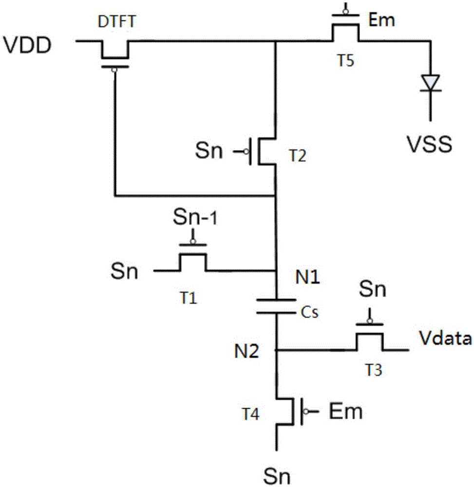
[0038] The display panel according to the embodiment of the present invention includes a plurality of gate scan lines, a plurality of data lines, and a plurality of pixel circuits arranged on a display substrate and arranged on a display substrate. The pixel circuits are formed on two adjacent gates. In the pixel area defined by the scan line and the two data lines, such as figure 1 As shown, the pixel circuit includes:

[0039] Storage ca...


PUM


Abstract

The invention provides a display panel, a driving method thereof and a display device with the display panel. A pixel circuit in the display panel comprises the components of a storage capacitor; a driving transistor; an initializing module which controls a gate scan line of this grade in an initializing time period for supplying an initial voltage for the first end of the storage capacitor; a compensating module; a data write-in module; a reset module which controls for realizing conduction between the gate scan line of this grade with the second end of the storage capacitor in a light emitting time period; and a light emitting control mold. The driving transistor is conducted in the light emitting time period for driving a light emitting element to emit light. The driving transistor is conducted in the light emitting time period for driving the light emitting element to emit light. The display panel, the driving method thereof and the display device with the display panel settles a problem of lighting brightness non-uniformness of the light emitting element caused by threshold voltage offset of the driving transistor and IR voltage drop of a power line. The gate scan line of this grade is used for supplying the initial voltage and a reset voltage. The display panel, the driving method and the display device with the display panel have advantages of effectively utilizing a gate scanning signal of this grade, reducing number of wirings in a pixel space, and facilitating realization of high-resolution display.

Description

Technical field [0001] The present invention relates to the field of display technology, in particular to a display panel, a driving method thereof, and a display device. Background technique [0002] In recent years, conventional display panels have been gradually replaced by portable flat display panels. The organic light-emitting display panel has attracted more attention due to its high brightness, wide viewing angle, good contrast, low power consumption, and high-speed response speed. [0003] However, when AMOLED (Active-matrix organic light emitting diode, active matrix organic light emitting diode) display panels develop to high resolution, due to the reduction of pixel area, insufficient wiring space has become the biggest problem in the industry, especially in the pixel circuit of thin film transistors. When the number cannot be reduced, reducing the power cord opens up another trend. In addition, due to the impact of the LTPS (Low Temperature Poly-silicon, low temperat...

Claims


Application Information

Patent Timeline
Patent Type & Authority Applications(China)
IPC IPC(8): G09G3/32
CPCG09G3/3233G09G3/3266G09G3/3291G09G2300/0819G09G2300/0842G09G2300/0861G09G2310/0251G09G2310/0262G09G2310/08G09G2320/0233G09G2300/043G09G2310/0202
Inventor 朱健超
Owner BOE TECH GRP CO LTD
Why Eureka
Try Eureka