
Pixel compensation circuit, driving method thereof and display device

A compensation circuit and pixel technology, applied in static indicators, instruments, etc., can solve the problems of reducing the uniformity of light-emitting element luminous brightness, unable to compensate the IR voltage drop of the power supply, and unstable light-emitting elements, so as to improve the display effect and eliminate the brightness Uneven, improved effect of impact

Active Publication Date: 2021-01-01
FUZHOU BOE OPTOELECTRONICS TECH CO LTD +1
View PDF14 Cites 4 Cited by
  • Summary
  • Abstract
  • Description
  • Claims
  • Application Information

AI Technical Summary

Problems solved by technology

Since the threshold voltage Vth of the driving transistor T2 is prone to drift and cannot compensate for the IR drop of the power supply, the driving current I of the light-emitting element OLED Unstable, which reduces the uniformity of the light-emitting brightness of the light-emitting element, thereby reducing the display effect

Method used


Image

  • Pixel compensation circuit, driving method thereof and display device
  • Pixel compensation circuit, driving method thereof and display device
  • Pixel compensation circuit, driving method thereof and display device

Examples


Embodiment Construction

[0038] The following will clearly and completely describe the technical solutions in the embodiments of the present invention with reference to the accompanying drawings in the embodiments of the present invention. Obviously, the described embodiments are only some, not all, embodiments of the present invention. Based on the embodiments of the present invention, all other embodiments obtained by persons of ordinary skill in the art without making creative efforts belong to the protection scope of the present invention.

[0039] In the embodiments of the present invention, words such as "first", "second", "third", "fourth" and "fifth" are used to distinguish the same or similar items with basically the same function and effect, The technical solutions of the embodiments of the present invention are only clearly described, and should not be understood as indicating or implying relative importance or implicitly indicating the quantity of the indicated technical features.

[0040]...


PUM


Abstract

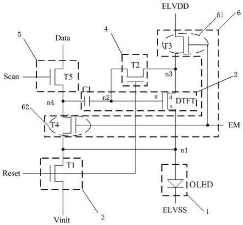
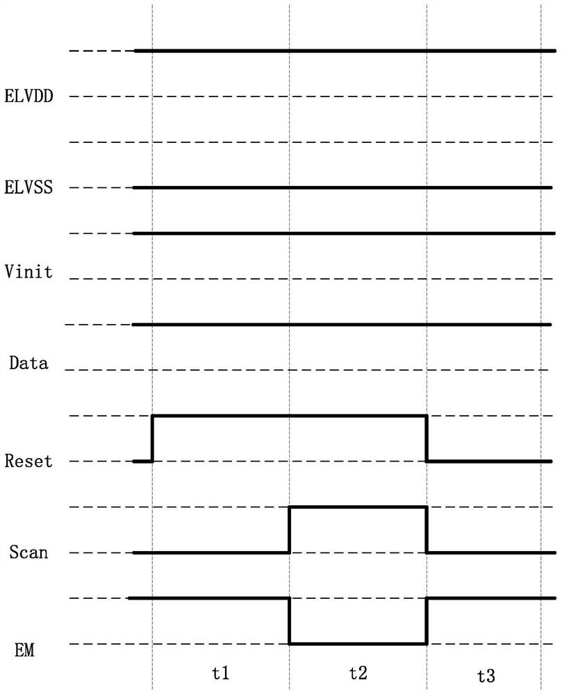
The invention provides a pixel compensation circuit, a driving method thereof and a display device, and relates to the technical field of display. The compensation circuit can eliminate the uneven brightness phenomenon of a light-emitting element caused by Vth drift, thereby improving the display effect. The circuit includes: the light-emitting element; a driving module which is electrically connected with a first node, a second node and a third node; reset modules, wherein the first reset module is electrically connected with a reset signal line, the first node and an initial signal line, andthe second reset module is electrically connected with the reset signal line, the second node and the third node; an input control module which is electrically connected with a scanning signal line,a data signal line and a fourth node; and light-emitting control modules, wherein the first light-emitting control module is electrically connected with a light-emitting control signal line, a secondpower signal line and the third node, the second light-emitting control module is electrically connected with the light-emitting control signal line, the first node and the fourth node, and the firstnode is electrically connected with an anode. The invention is suitable for manufacturing the pixel compensation circuit.

Description

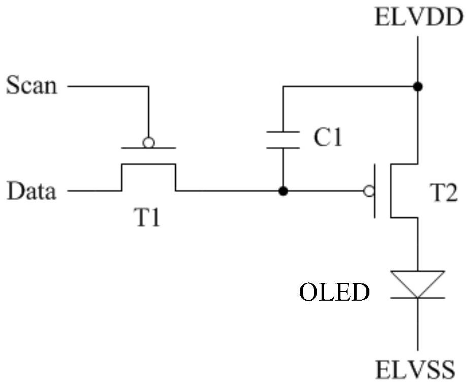
technical field [0001] The invention relates to the field of display technology, in particular to a pixel compensation circuit, a driving method thereof, and a display device. Background technique [0002] The OLED (Organic Light Emitting Diode, Organic Light Emitting Diode) display device has the advantages of wide color gamut, high contrast, energy saving, foldable, etc., and has strong competitiveness in various display devices. Among them, the AMOLED (Active-Matrix Organic Light Emitting Diode, Active-Matrix Organic Light Emitting Diode) display device is one of the key development directions in the OLED display device. [0003] figure 1 Shown is a pixel compensation circuit of an AMOLED display device in the related art, including a switching transistor T1, a driving transistor T2, a storage capacitor C1 and a light emitting element OLED. The driving current of the light-emitting element OLED is controlled by the driving transistor T2, and its current size is: I OLED...

Claims


Application Information

Patent Timeline
Patent Type & Authority Applications(China)
IPC IPC(8): G09G3/3225
CPCG09G3/3225G09G2320/0233
Inventor 翁祖伟翁彬黄宇鹏刘葆黄巧红
Owner FUZHOU BOE OPTOELECTRONICS TECH CO LTD
Learn More