Pixel circuit, driving method and display device

A technique for pixel circuits and drive transistors, applied in the field of drive methods, display devices, and pixel circuits, capable of solving problems such as uneven pixel brightness and uneven luminous brightness

Inactive Publication Date: 2019-12-27
BOE TECH GRP CO LTD
View PDF18 Cites 5 Cited by
  • Summary
  • Abstract
  • Description
  • Claims
  • Application Information

AI Technical Summary

Problems solved by technology

[0003] Embodiments of the present invention provide a pixel circuit, a driving method, and a display device, which are used to solve the problems of uneven brightness of each pixel and uneven overall luminous brightness in the display device.

Method used


Image

  • Pixel circuit, driving method and display device
  • Pixel circuit, driving method and display device
  • Pixel circuit, driving method and display device

Examples


Embodiment 1

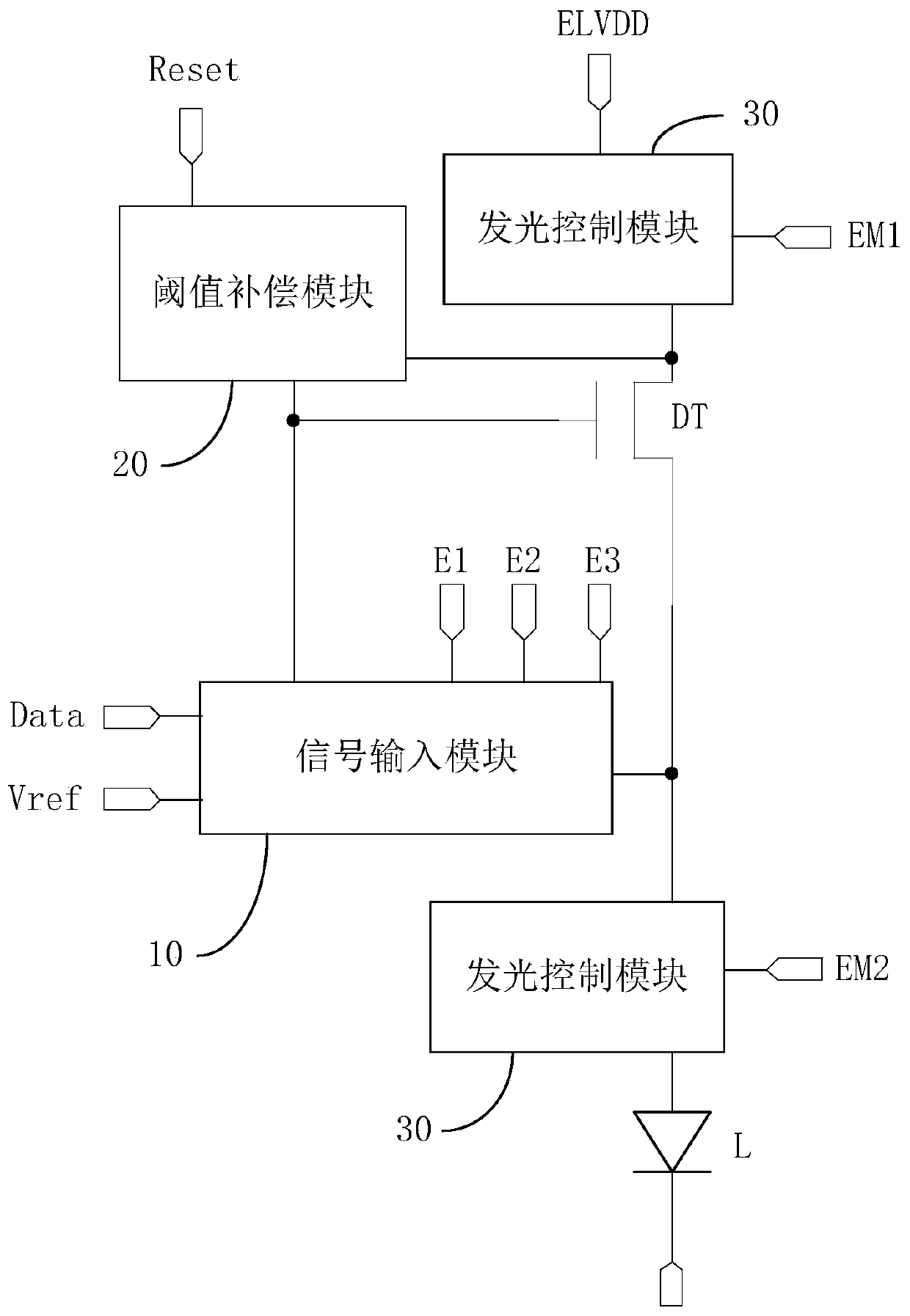
[0058] In specific implementation, in the pixel circuit provided by the embodiment of the present invention, such as image 3 , Figure 4 , Figure 8 As shown, the driving transistor DT can be an N-type transistor. For the case where the driving transistor DT is a P-type transistor, the design principle is the same as that of the present invention, and also belongs to the protection scope of the present invention.

[0059] During specific implementation, in the pixel circuit provided by the embodiment of the present invention, the first terminal of the light emitting device L is electrically connected to the light emitting control module, and the second terminal of the light emitting device L is electrically connected to the second power supply terminal ELVSS. Moreover, in specific implementation, the light emitting device L may be at least one of: organic light emitting diodes (Organic Light Emitting Diode, OLED) and quantum dot light emitting diodes (Quantum Dot Light Emitt...

Embodiment 2

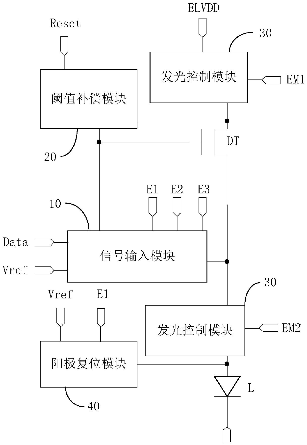
[0095] The schematic structural diagram of the pixel circuit corresponding to the embodiment of the present invention is as follows Figure 5 As shown, some implementations of the above-mentioned embodiments are modified. The following only describes the differences between this embodiment and the above-mentioned embodiments, and the similarities will not be repeated here.

[0096] In specific implementation, in the pixel circuit provided by the embodiment of the present invention, such as Figure 5 As shown, the signal input module 10 may also include: a fourth switching transistor T4, a fifth switching transistor T5, a sixth switching transistor T6, and a second capacitor C2; wherein,

[0097] The gate of the fourth switching transistor T4 is electrically connected to the first control signal terminal E1, the first pole is electrically connected to the data signal terminal Data, and the second pole is respectively connected to the first pole of the second capacitor C2 and t...

Embodiment 3

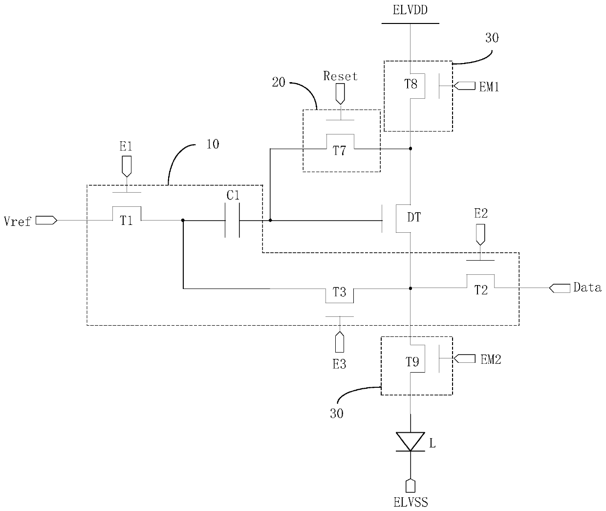
[0113] by Figure 4 The pixel circuit shown as an example, combined with the circuit signal timing Figure 10 The working process of the above-mentioned pixel circuit provided by the embodiment of the present invention is described. The following only describes the differences between this embodiment and the above-mentioned embodiments, and the similarities will not be repeated here.

[0114] Specifically, choose the Figure 10 The three stages of t1, t2 and t3 in the input timing diagram shown. Such as Figure 4 As shown, the reset signal terminal Reset and the first control signal terminal E1 and the second control signal terminal E2 may be the same terminal; the second light emission control signal terminal EM2 and the third control signal terminal E3 may be the same terminal.

[0115] In the t1 stage, Reset=1, EM1=1, EM2=0.

[0116] Since Reset=1, the tenth switching transistor T10 is turned on, so the voltage VREF of the reference signal terminal Vref is output to th...


PUM


Abstract

The invention discloses a pixel circuit, a driving method and a display device. The pixel circuit comprises a signal input module, a threshold compensation module, a light-emitting control module, a driving transistor and a light-emitting device, the signal input module writes the voltage of the data signal end, the voltage of the reference voltage signal end and the threshold voltage of the driving transistor into the grid electrode of the driving transistor according to the signals of the first, second and third control signal ends; the threshold compensation module is used for conducting the grid electrode of the driving transistor with the first electrode of the driving transistor under the control of a signal of a reset signal end; the light-emitting control module is controlled by the first light-emitting control end and the second light-emitting control end to conduct the first power supply end and the driving transistor and conduct the driving transistor and the light-emittingdevice, so that the light-emitting device emits light. Through the mutual cooperation of the modules and the elements, the problem of non-uniform luminance caused by non-uniform threshold voltage andvoltage drop of the first power supply end is solved.

Description

technical field [0001] The invention relates to the field of display technology, in particular to a pixel circuit, a driving method and a display device. Background technique [0002] The organic light emitting diode (Organic Light Emitting Diode, OLED) panel has the characteristics of bendability, high contrast ratio, low power consumption, etc., and has received extensive attention. Among them, the pixel circuit is the core technical content of the OLED panel, which has important research significance. Generally, the OLED in the OLED panel is driven to emit light by the current generated by the driving transistor in the pixel circuit. However, due to the limitation of the process and the increase of the service time, the threshold voltage Vth of the driving transistor will drift to different degrees, so that the OLED panel will have the problem of uneven luminance of the OLED. Moreover, due to the existence of IRDrop (voltage drop) in the OLED panel, the OLED panel will ...

Claims


Application Information

Patent Timeline
Patent Type & Authority Applications(China)
IPC IPC(8): G09G3/3258
CPCG09G3/3258G09G2320/0233G09G3/3233G09G2300/0819G09G2300/0842G09G2300/0861G09G2320/0238G09G2320/0223G09G2310/061G09G2310/08
Inventor 董甜
Owner BOE TECH GRP CO LTD
Why Eureka
Try Eureka