Semiconductor packaging structure and packaging method

A technology of packaging structure and packaging method, applied in semiconductor devices, semiconductor/solid-state device manufacturing, semiconductor/solid-state device components and other directions, can solve the problems of unequal volume, open-circuit pillow effect failure, vertical chip fracture, etc.

Active Publication Date: 2015-11-25
TSINGHUA UNIV
View PDF7 Cites 5 Cited by
  • Summary
  • Abstract
  • Description
  • Claims
  • Application Information

AI Technical Summary

Problems solved by technology

However, in the above two packaging technologies, due to the difference in coefficient of thermal expansion (CTE) between the material of the packaging layer 20 (for example, EMC) and the substrate material (for example, FR4 or BT) (for example, the thermal expansion coefficient of a certain EMC is 45ppm, while the thermal expansion coefficient of FR4 used for the substrate is 18ppm), which leads to the unequal expansion volume of the packaging layer 2

Method used


Image

  • Semiconductor packaging structure and packaging method
  • Semiconductor packaging structure and packaging method
  • Semiconductor packaging structure and packaging method

Examples


Embodiment Construction

[0043] Specific embodiments of the present invention will be described in detail below in conjunction with the accompanying drawings. It should be understood that the specific embodiments described here are only used to illustrate and explain the present invention, and are not intended to limit the present invention.

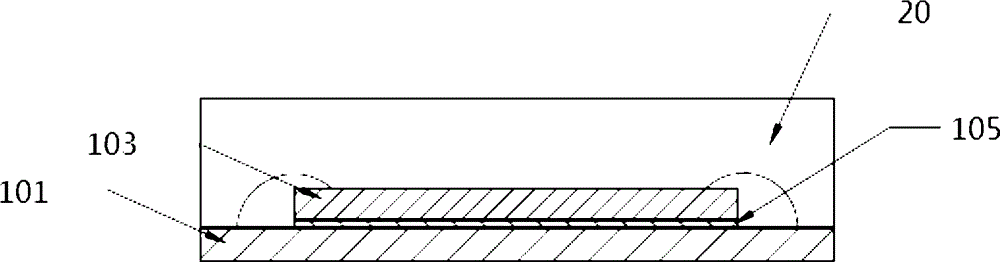
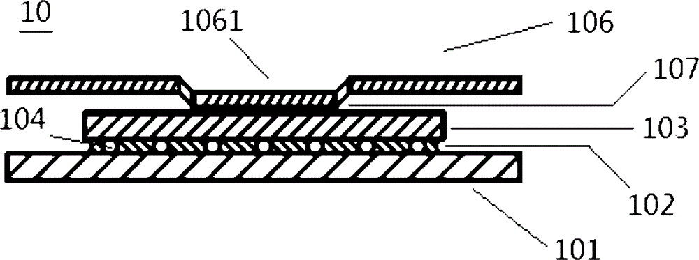
[0044] figure 2 and image 3 A schematic structural diagram of a semiconductor package structure according to two implementations of the present invention is shown. Such as figure 2 and image 3 As shown, the semiconductor package structure 10 may include: a substrate 101, a chip 103 located on the substrate 101 and electrically connected to the substrate 101, and a packaging layer for packaging the chip 103 (although in figure 2 and image 3 It is not shown in , but it can be understood that the encapsulation layer can be, for example, the encapsulation layer 20 shown in FIG. 1).

[0045] figure 2 An example of realizing the electrical connection bet...


PUM


Abstract

The invention discloses a semiconductor packaging structure and a packaging method. the packaging structure comprises a substrate, at least one chip located on the substrate and electrically connected with the substrate, a packaging layer for packaging the at least one chip, and a frame fixed on the upper surface of one chip and upper surfaces of the multiple chips, wherein the frame has a smaller thermal expansion coefficient that the packaging layer. Through fixing the frame on the upper surface of the chip, symmetry of the packaging structure can be added. As the frame has a smaller thermal expansion coefficient that the packaging layer, the thermal expansion coefficient of the packaging layer can be effectively reduced as the frame is additionally arranged. Thus, in the case of temperature rise and fall, the packaging layer and the substrate have basically the same expansion volumes. Warping caused by the thermal expansion coefficient difference can be effectively reduced, the chip can be prevented from being broken, and reliability of the packaging structure is improved.

Description

technical field [0001] The present invention relates to the field of semiconductor packaging, in particular to a semiconductor packaging structure and packaging method. Background technique [0002] There are two main traditional packaging technologies, one is flip-chip bonding (that is, Flip-Chip - flip-chip welding chip), the other is wire bonding (Wirebond), respectively, as Figure 1a and Figure 1b shown. [0003] exist Figure 1a In the illustrated flip-chip packaging technology, a plurality of solder balls 104 are implanted between the chip 103 and the substrate 101 , and the underfill 102 is filled to realize the electrical connection between the chip 103 and the substrate 101 . Afterwards, the chip 103 is packaged with the packaging layer 20 . Wherein, the material of the encapsulation layer 20 may be, for example, molding compound (EMC). exist Figure 1b In the wire bonding packaging technology shown, the chip 103 is pasted on the substrate 101 by using the adh...

Claims


Application Information

Patent Timeline
IPC IPC(8): H01L23/24H01L21/50
CPCH01L2224/16225H01L2224/48091H01L2224/48227H01L2224/73204H01L2224/73253H01L2224/73265H01L2924/181H01L2924/00014H01L2924/00012
Inventor 蔡坚陈钏谭琳王谦
Owner TSINGHUA UNIV
Why Eureka
Try Eureka