Integrated device of awg output waveguide and waveguide detector and its preparation method

An output waveguide and integrated device technology, applied in the field of optoelectronic devices and their integration, can solve problems such as high coupling energy consumption, poor system stability, and impact on applications, and achieve the effects of simplifying device packaging, reducing process requirements, and improving stability

Active Publication Date: 2018-03-06
INST OF SEMICONDUCTORS - CHINESE ACAD OF SCI
View PDF4 Cites 0 Cited by
  • Summary
  • Abstract
  • Description
  • Claims
  • Application Information

AI Technical Summary

Problems solved by technology

[0004] In the process of realizing the present invention, the applicant found that in the prior art, the AWG output waveguide and the waveguide detector are set separately, the stability of the system is poor, and the coupling energy consumption is high, which affects the application of the two in the field of optical communication.

Method used


Image

  • Integrated device of awg output waveguide and waveguide detector and its preparation method
  • Integrated device of awg output waveguide and waveguide detector and its preparation method
  • Integrated device of awg output waveguide and waveguide detector and its preparation method

Examples


Embodiment Construction

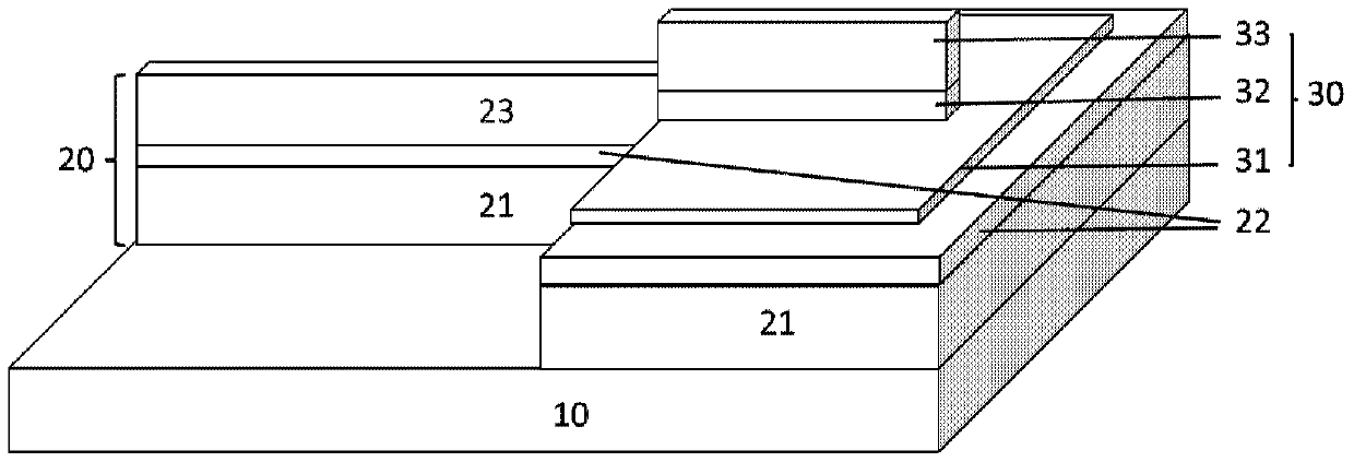
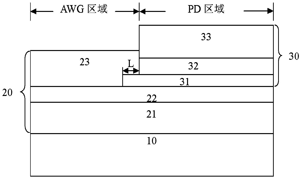
[0032] In the present invention, the main structure of the device is constructed by semiconductor technology, and the compatibility of the AWG and the waveguide detector epitaxial structure is realized through the secondary epitaxy technology, and the seamless connection of the two increases the alignment tolerance of the detector mesa etching, At the same time, the coupling energy consumption is reduced.

[0033] In order to make the object, technical solution and advantages of the present invention clearer, the present invention will be described in further detail below in conjunction with specific embodiments and with reference to the accompanying drawings.

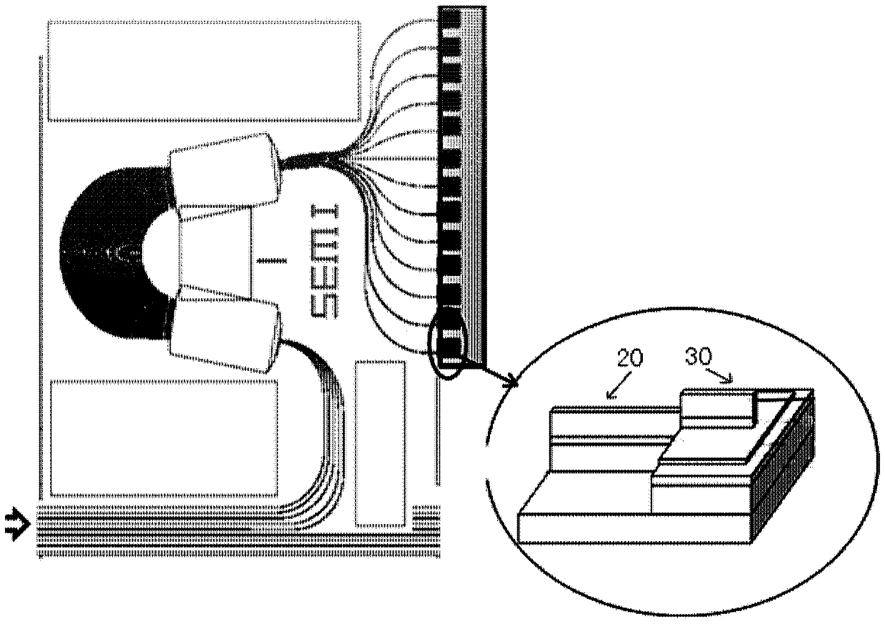
[0034] In an exemplary embodiment of the present invention, an integrated device of an AWG output waveguide and a waveguide detector is provided. Figure 1A It is a perspective view of an integrated device of an AWG output waveguide and a waveguide detector according to an embodiment of the present invention. Figure 1...


PUM


Abstract

The invention provides an AWG output waveguide and waveguide detector integration device and a preparation method thereof. The integration device comprises a substrate, an AWG output waveguide and a waveguide detector, and is characterized in that the AWG output waveguide is strip-shaped and located in an AWG area on the substrate, the AWG output waveguide comprises an AWG lower covering layer, an AWG core layer and an AWG upper covering layer from the bottom up, and the AWG lower covering layer and the AWG core layer extend to a PD area; and the waveguide detector is formed above the AWG cover layer of the PD area on the substrate and is arranged opposite to the AWG output waveguide, and the waveguide detector comprises a PD lower contact layer, a PD absorbing layer and a PD upper contact layer from the bottom up. According to the invention, light transmitted in the AWG output waveguide is coupled to the PD absorbing layer of the waveguide detector layer by layer from the AWG core layer in a mode of evanescent field coupling from the bottom up, thereby avoiding excessive coupling loss in interconnection of discrete devices, and improving the energy efficiency in an optical link by using evanescent field coupling.

Description

technical field [0001] The invention relates to the field of optoelectronic devices and their integration, in particular to an integrated device of an AWG output waveguide and a waveguide detector and a preparation method thereof. Background technique [0002] The emergence of various information networks covering the whole world marks the entry of human beings into the information society. With the development of society, people's demand for information services is increasing day by day, and correspondingly, the bandwidth of the communication system is required to increase continuously. In order to meet the increasing transmission traffic in the world, the process of intelligent optical network characterized by all-optical information processing and information service broadband represented by fiber-to-the-home is accelerating. A new generation of optical fiber communication evolution with integration, low cost and high reliability. The wavelength division multiplexing (W...

Claims


Application Information

Patent Timeline
Patent Type & Authority Patents(China)
IPC IPC(8): G02B6/12G02B6/13
CPCG02B6/12009G02B6/131G02B6/136
Inventor 吕倩倩韩勤杨晓红尹伟红
Owner INST OF SEMICONDUCTORS - CHINESE ACAD OF SCI
Why Eureka
Try Eureka