Preparation method of silicon waveguide and silicon oxide waveguide mode converter

A mode converter and silicon waveguide technology, applied in the fields of optical sensing and optical communication, can solve the problems of Fresnel reflection loss, unsuitable for batch packaging, end-face coupling mode mismatch, etc., so as to solve the coupling loss and meet the energy conversion requirements. The effect of efficiency

Active Publication Date: 2022-07-19
CHANGCHUN UNIV OF SCI & TECH
View PDF5 Cites 0 Cited by
  • Summary
  • Abstract
  • Description
  • Claims
  • Application Information

AI Technical Summary

Problems solved by technology

[0004] However, product development based on SOI technology has shown that this technology also has its inherent shortcomings
The large refractive index difference between the core layer and the cladding layer causes the end-face coupling mode mismatch between the waveguide chip and the fiber, which results in a very low coupling efficiency problem between the photonic integrated circuit chip and the fiber; the waveguide core layer and the fiber The excessive refractive index difference of the fiber core layer also causes Fresnel reflection loss, so it has been a key technical issue in this field for more than 20 years.
At present, the guided wave mode conversion based on physics is widely used. There are two representative technologies: 1. Design and process the longitudinal coupling grating structure at the output end of the waveguide to achieve more effective waveguide-fiber end-face coupling. However, this process The technology is difficult, and so far there is no research report on the coupling loss of <1.0dB / facet; 2. Design the output end of the waveguide into a trapezoidal shape and make an end-face coupling grating, and then the end face of the fiber is coupled with the grating from the chip. The technology enables the optical fiber and the waveguide to be on different planes, which is suitable for laboratory testing, but not suitable for batch packaging. Moreover, there has been no research report on the coupling loss of <1.0dB / facet so far.
Therefore, the coupling loss between waveguide chips and optical fibers has always been the "bottleneck" problem that limits silicon waveguide integrated devices from laboratory to industrialization.

Method used


Image

  • Preparation method of silicon waveguide and silicon oxide waveguide mode converter
  • Preparation method of silicon waveguide and silicon oxide waveguide mode converter
  • Preparation method of silicon waveguide and silicon oxide waveguide mode converter

Examples


Embodiment Construction

[0028] The present invention will be further described in detail below with reference to the accompanying drawings and embodiments.

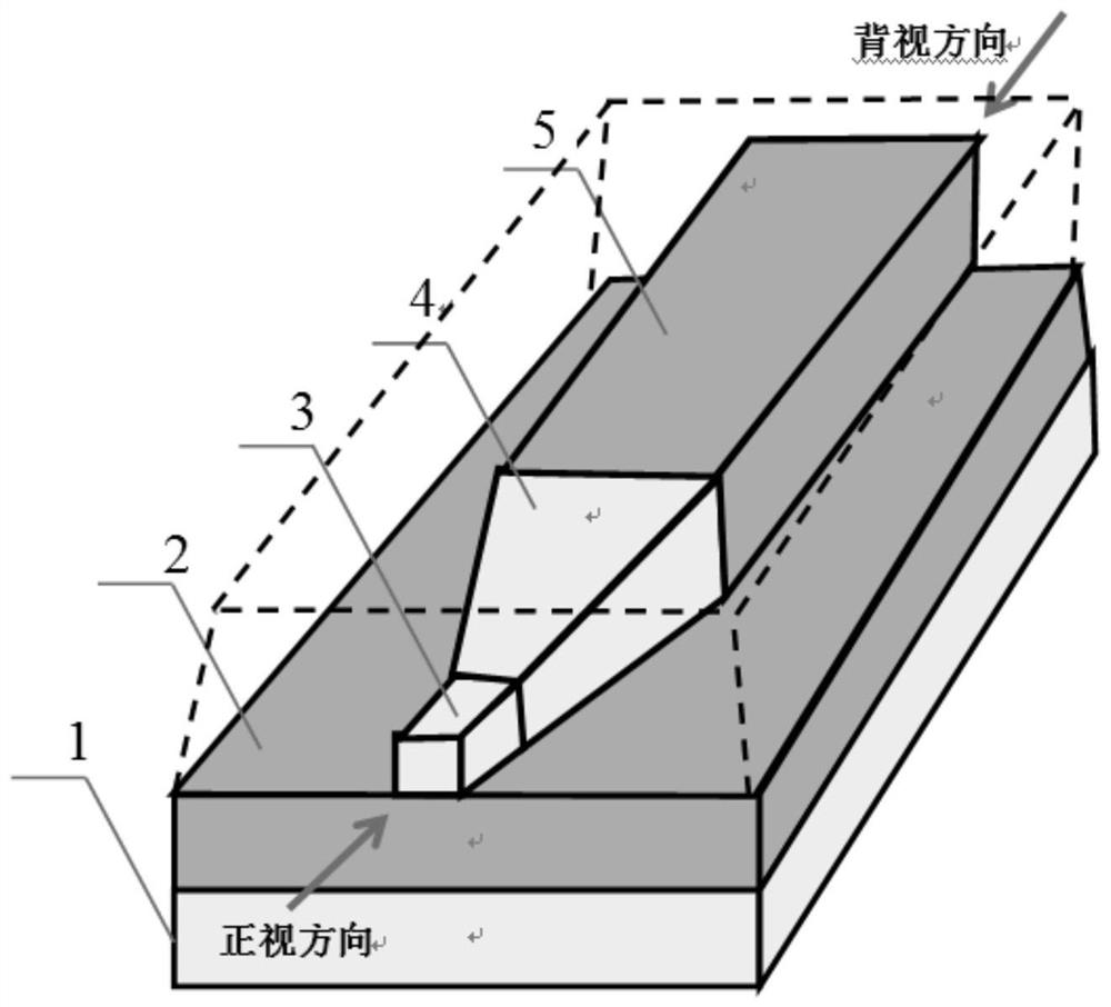
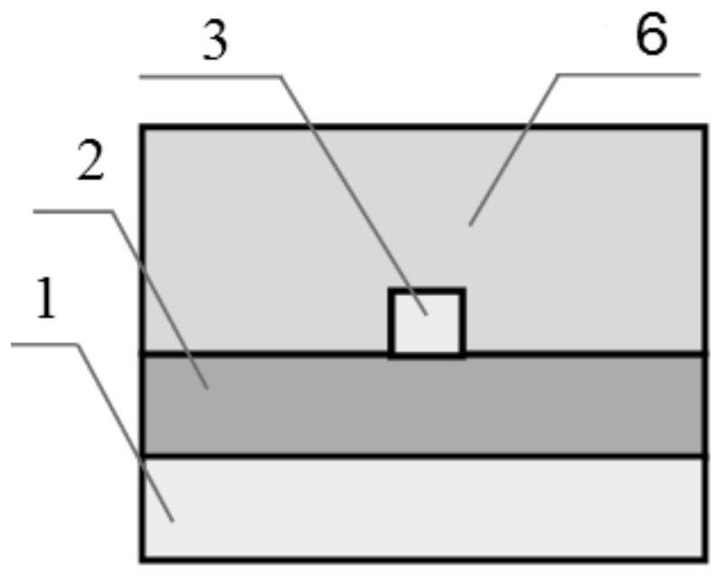
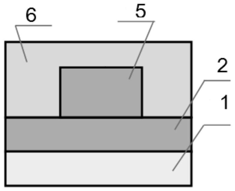
[0029] like figure 1 As shown, a silicon waveguide and a silicon oxide waveguide mode converter, the converter includes: a silicon substrate 1, a silicon dioxide bottom cladding layer 2, a single-mode silicon waveguide core 3, a wedge-shaped waveguide core 4, and a single-mode silicon dioxide waveguide core 5 and the silicon dioxide upper cladding layer 6; the silicon dioxide bottom cladding layer 2 is arranged on the silicon substrate 1, and the single-mode silicon waveguide core 3, Wedge-shaped waveguide core 4 and single-mode silica waveguide core 5; the single-mode silicon waveguide core 3, wedge-shaped waveguide core 4 and single-mode silica waveguide core 5 are integrated structures, and the wedge-shaped waveguide core 4 is close to the The part of the single-mode silicon waveguide core 3 is a silicon waveguide core, and the part close to...


PUM

PropertyMeasurementUnit
thicknessaaaaaaaaaa
widthaaaaaaaaaa

Abstract

A silicon waveguide and silicon oxide waveguide mode converter and a preparation method thereof relate to the technical field of optical communication and optical sensing. The converter includes: a silicon substrate, a silicon dioxide bottom cladding layer, a single-mode silicon waveguide core, a wedge-shaped waveguide core, The silicon oxide waveguide core and the silicon dioxide upper cladding layer; the silicon dioxide bottom cladding layer is provided on the silicon substrate, and the single-mode silicon waveguide core, the wedge-shaped waveguide core and the single-mode silicon waveguide core are sequentially arranged on the silicon dioxide bottom cladding layer from one end to the other end. Mode silica waveguide core; single-mode silicon waveguide core, wedge-shaped waveguide core and single-mode silica waveguide core are integrated structure, single-mode silica waveguide core is strip structure; wedge-shaped waveguide core is close to single-mode silicon waveguide core The part of the silicon waveguide core is the silicon waveguide core, and the part close to the single-mode silicon dioxide waveguide core is the silicon dioxide waveguide core. Through this method, the conversion effect from single mode to single mode is achieved, that is, the mode conversion in the waveguide between the silicon single mode waveguide and the silicon oxide single mode waveguide is realized, and the energy conversion efficiency between the waveguide and the optical fiber is finally satisfied.

Description

technical field [0001] The invention relates to the technical field of optical communication and the technical field of optical sensing, in particular to a silicon waveguide and silicon oxide waveguide mode converter and a preparation method thereof. Background technique [0002] At present, the capacity and speed of optical communication networks are growing rapidly, which requires the transmission and processing of data with a large amount of information. Cloud computing also puts forward higher and higher requirements for the capacity and speed of computers. Therefore, the data transmission and storage of computers make electronic The thermal energy consumption and electromagnetic interference caused by the large amount of information carried by the circuit chip are the main pressures faced by the next-generation computers. In modern optical fiber communication systems, whether it is based on the planar lightwave circuit (PLC) technology based on silicon oxide on silicon ...

Claims


Application Information

Patent Timeline
Patent Type & Authority Patents(China)
IPC IPC(8): G02B6/14G02B6/30
CPCG02B6/14G02B6/305
Inventor 孙德贵于汀
Owner CHANGCHUN UNIV OF SCI & TECH
Why Eureka
Try Eureka