Packaging method and packaging structure thereof

A technology of packaging structure and packaging method, applied in the direction of coupling of optical waveguides, can solve problems such as affecting the transmission quality of optical communication links and increasing coupling loss, etc.

Pending Publication Date: 2022-04-05
WUHAN OPTICAL VALLEY INFORMATION OPTOELECTRONICS INNOVATION CENT CO LTD +1
View PDF5 Cites 0 Cited by
  • Summary
  • Abstract
  • Description
  • Claims
  • Application Information

AI Technical Summary

Problems solved by technology

In this way, the coupling loss is increased, which affects the transmission quality of the optical communication link between optical devices

Method used


Image

  • Packaging method and packaging structure thereof
  • Packaging method and packaging structure thereof
  • Packaging method and packaging structure thereof

Examples


Embodiment Construction

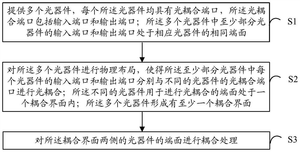
[0031] In order to make the technical solutions and advantages of the embodiments of the present invention clearer, the technical solutions of the present invention will be further described in detail below in conjunction with the accompanying drawings and specific embodiments.

[0032] The term "optical device" as used in the following description may include structures of active and passive devices with light-conducting media, including but not limited to integrated optoelectronic chips, silicon-based optoelectronic chips, silicon-based optical waveguides, optoelectronic Chips, optical switches, optical waveguides, multimode interference (MMI) optical couplers, optical filters, and optical modulators.

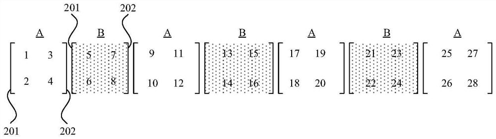
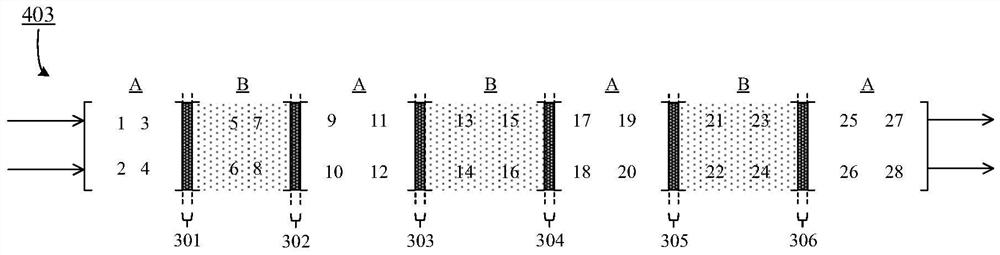
[0033] In the design of an integrated optoelectronic chip, there are usually multiple different optical devices that need to be connected. A typical situation is that two different optical devices need to be connected alternately, resulting in multiple coupling interfaces that...


PUM


Abstract

The embodiment of the invention provides a packaging method and a packaging structure thereof, and the packaging method comprises the steps: a plurality of optical devices are provided, each optical device is provided with an optical coupling port, and the optical coupling port comprises an input port and an output port; the input ports and the output ports of at least part of the optical devices in the plurality of optical devices are located on the same end face of the corresponding optical devices; performing physical layout on the plurality of optical devices, so that the input port and the output port of each optical device in the at least part of optical devices are optically coupled with the optical coupling ports of different optical devices respectively; the end faces, used for optical coupling, of the different optical devices are located in a coupling interface. The plurality of optical devices form at least one coupling interface; and carrying out coupling processing on the end surfaces of the optical devices on the two sides of the coupling interface.

Description

technical field [0001] The invention relates to the technical field of optical communication devices, in particular to a packaging method and a packaging structure thereof. Background technique [0002] In system-level design, there are usually multiple different optical devices that need to be connected. In a typical situation, two different optical devices need to be connected alternately. At this time, multiple coupling interfaces will be generated and multiple couplings will be performed. However, multiple couplings require repeated placing of the optical device on the bench and repeated coupling of the package. In this way, the coupling loss is increased, which affects the transmission quality of the optical communication link between the optical devices. Contents of the invention [0003] In order to solve related technical problems, an embodiment of the present invention proposes a packaging method and a packaging structure thereof. [0004] An embodiment of the p...

Claims


Application Information

Patent Timeline
IPC IPC(8): G02B6/42
Inventor 常思垚钱懿王磊傅焰峰徐路
Owner WUHAN OPTICAL VALLEY INFORMATION OPTOELECTRONICS INNOVATION CENT CO LTD
Why Eureka
Try Eureka