Pulse width modulation system control method and misoperation prevention circuit therefor

A technology of pulse width modulation and control method, which is applied in pulse duration/width modulation, logic circuit, pulse technology, etc., can solve problems such as the damage of the post-stage circuit 14 and the abnormal operation of the post-stage circuit 14, so as to avoid abnormality effect of action

Active Publication Date: 2015-12-23
DELTA ELECTRONICS INC
View PDF4 Cites 0 Cited by
  • Summary
  • Abstract
  • Description
  • Claims
  • Application Information

AI Technical Summary

Problems solved by technology

When the output voltage ΔV of the microprocessor 11 changes from the first time point (t 1 ) when 0V climbs to the third point (t 3 ) and reach the required voltage level and complete the voltage establishment, during the rising period of the output voltage ΔV, the output voltage ΔV of the microprocessor 11 may be lower than the voltage judgment value set by the buffer circuit 12, for example Figure 2A As shown, when the output voltage ΔV of the microprocessor 11 has not yet reached the second specific voltage level V 2s When it is less than the voltage judgment value set by the buffer circuit 12, the buffer circuit 12 recognizes that both the input terminal 121 and the start terminal 122 are the forbidden level voltage (low level voltage), so the buffer circuit 12 is convenient for the output control terminal 123 to generate a forbidden voltage. Can level voltage V L (low level voltage), that is, the output control terminal 123 of the buffer circuit 12 is in the first period T 1 will generate the disable level voltage V L ,like Figure 2D As shown, in this way, the pulse width modulation system 1 will output the disable level voltage V when establishing the required voltage stages of the first module 113 and the second module 114 L As a result, the rear-stage circuit 14 operates abnormally, resulting in the risk of damage to the rear-stage circuit 14.

Method used


Image

  • Pulse width modulation system control method and misoperation prevention circuit therefor
  • Pulse width modulation system control method and misoperation prevention circuit therefor
  • Pulse width modulation system control method and misoperation prevention circuit therefor

Examples


Embodiment Construction

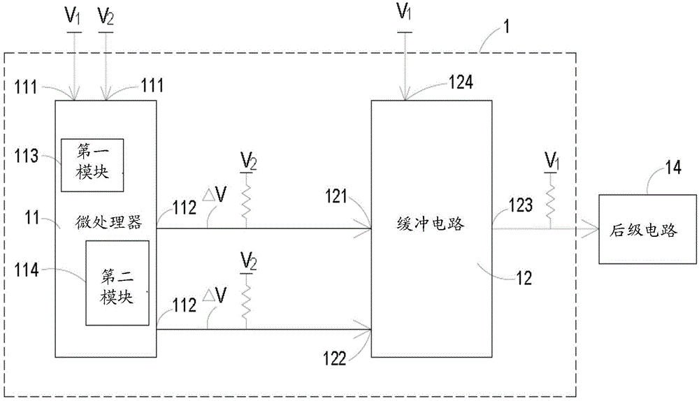
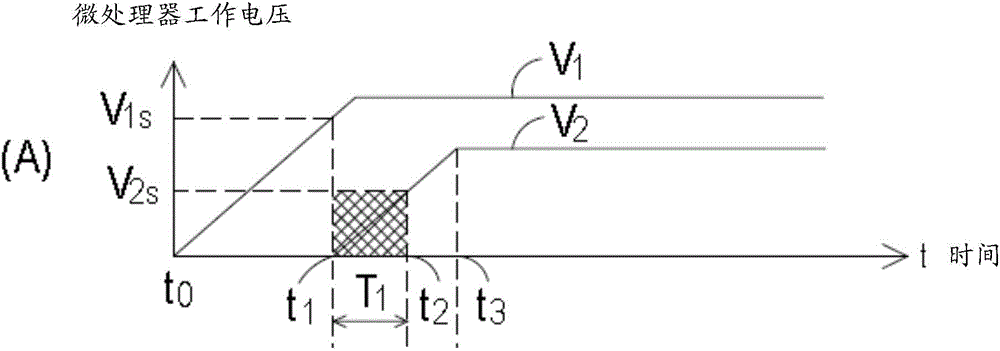
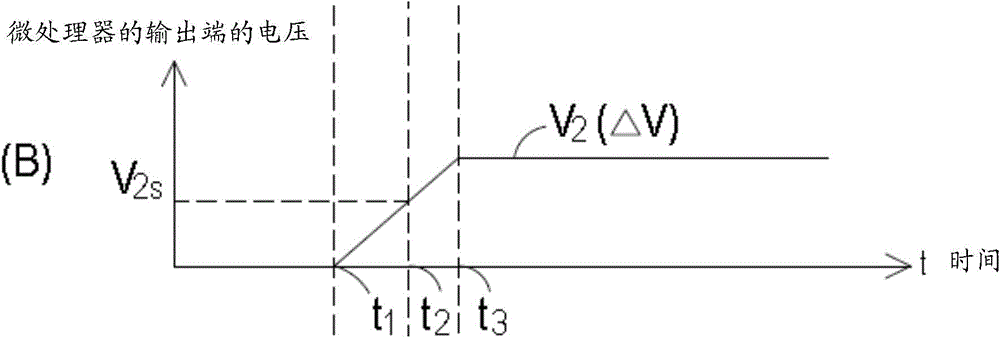
[0099] In order to make the purpose, technical solutions and advantages of the embodiments of the present invention clearer, the technical solutions in the embodiments of the present invention will be clearly and completely described below in conjunction with the drawings in the embodiments of the present invention. Obviously, the described embodiments It is a part of embodiments of the present invention, but not all embodiments. Elements and features described in one drawing or one embodiment of the present invention may be combined with elements and features shown in one or more other drawings or embodiments. It should be noted that representation and description of components and processes that are not related to the present invention and known to those of ordinary skill in the art are omitted from the drawings and descriptions for the purpose of clarity. Based on the embodiments of the present invention, all other embodiments obtained by persons of ordinary skill in the ar...


PUM


Abstract

The invention discloses a pulse width modulation system control method and a misoperation prevention circuit therefor. A pulse width modulation system comprises a microprocessor, a buffering circuit, and the misoperation prevention circuit. The misoperation prevention circuit is formed by that a power supply is connected between a first output end of the microprocessor and the starting end of the buffering circuit. The buffering circuit is provided with an output control end. The control method comprises steps: (a) sequentially supplying a first working voltage and a second working voltage to the microprocessor; (b) building a first output end corresponding to the second working voltage and building an output voltage in a process that the second working voltage rises to a needed voltage level from zero when the microprocessor receives the second working voltage; (c) enabling the output voltage to be converted into an enable voltage through the misoperation prevention circuit, and outputting the enable voltage to the starting end; (d) enabling the output control end to carry out high-impedance output according to the enable voltage of the starting end.

Description

technical field [0001] The present invention relates to a control method of a pulse width modulation system, especially a control method of a pulse width modulation system capable of preventing the abnormality of the subsequent circuit in the voltage stage required by the microprocessor to establish its own internal modules and its malfunction prevention circuit. Background technique [0002] The Pulse Width Modulation (PWM) system has been widely used in various electronic devices, such as motors, to control the operation of the electronic devices. When the traditional pulse width modulation system controls the operation of the subsequent circuit, it must first establish the corresponding working voltage for the corresponding modules inside the microprocessor when the microprocessor establishes the voltage stage required by each module in the microprocessor, and establishes During the process, the output terminals of the pulse width modulation system must maintain the enab...

Claims


Application Information

Patent Timeline
Patent Type & Authority Applications(China)
IPC IPC(8): H03K7/08H03K19/00
Inventor 江伯崧
Owner DELTA ELECTRONICS INC
Why Eureka
Try Eureka